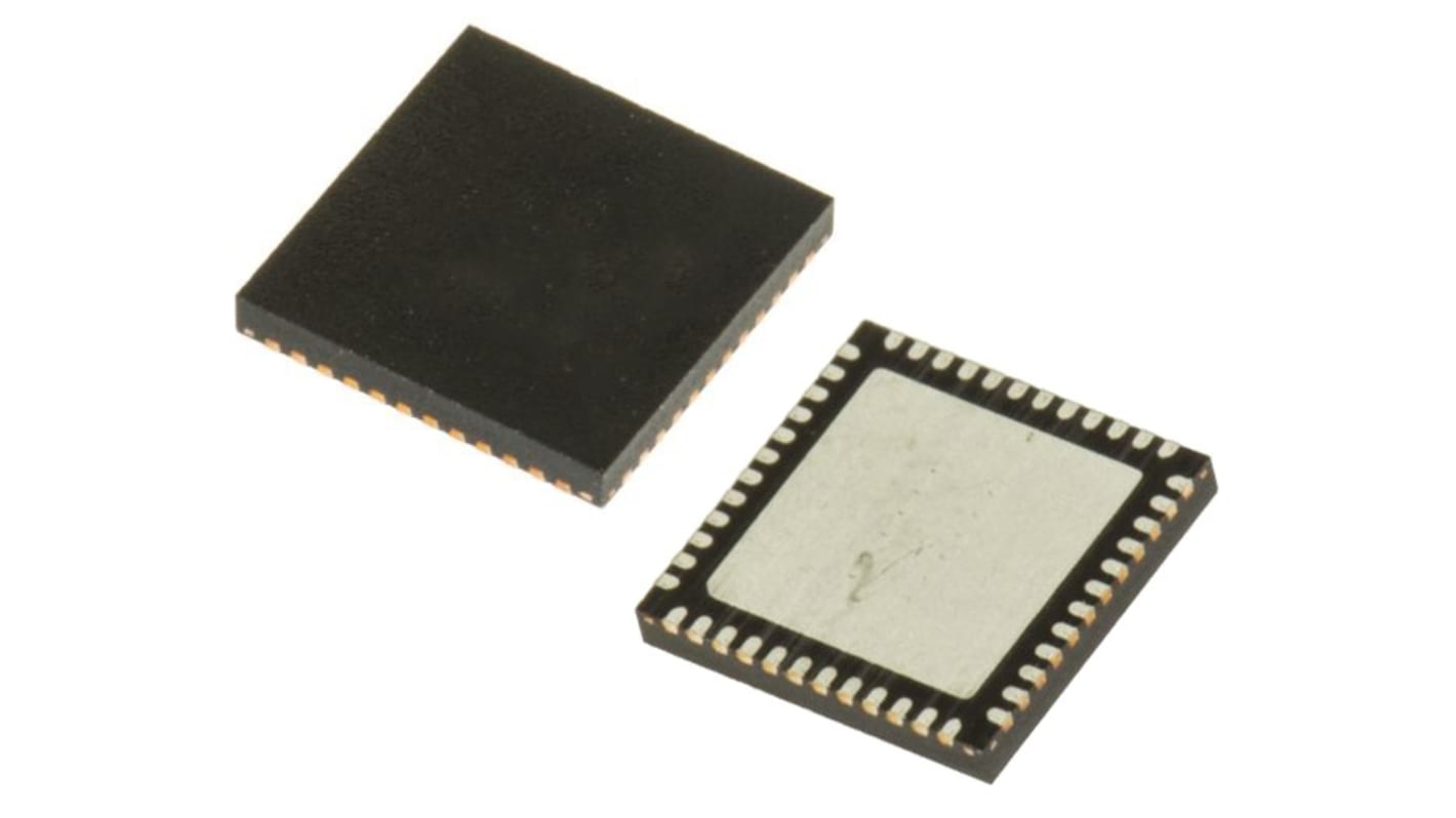
Renesas Electronics 8T39S11ANLGI Clock Buffer 48-Pin VFQFN-48
- RS Stock No.:
- 264-3519
- Mfr. Part No.:
- 8T39S11ANLGI
- Brand:
- Renesas Electronics

Currently unavailable
We don't know if this item will be back in stock, RS intend to remove it from our range soon.
- RS Stock No.:
- 264-3519
- Mfr. Part No.:
- 8T39S11ANLGI
- Brand:
- Renesas Electronics
Specifications
Technical Reference
Legislation and Compliance
Product Details
Find similar products by selecting one or more attributes.
Select all | Attribute | Value |
|---|---|---|
| Brand | Renesas Electronics | |
| Product Type | Clock Buffer | |
| Maximum Input Frequency | 40MHz | |
| Mount Type | Surface | |
| Maximum Propagation Delay Time | 2.65ns | |
| Package Type | VFQFN-48 | |
| Pin Count | 48 | |
| Minimum Supply Voltage | 2.5V | |
| Maximum Supply Voltage | 3.3V | |
| Minimum Operating Temperature | -40°C | |
| Maximum Operating Temperature | 85°C | |
| Standards/Approvals | RoHS | |
| Length | 7mm | |
| Series | 8T39S11A | |
| Height | 0.85mm | |
| Automotive Standard | No | |
| Select all | ||
|---|---|---|
Brand Renesas Electronics | ||
Product Type Clock Buffer | ||
Maximum Input Frequency 40MHz | ||
Mount Type Surface | ||
Maximum Propagation Delay Time 2.65ns | ||
Package Type VFQFN-48 | ||
Pin Count 48 | ||
Minimum Supply Voltage 2.5V | ||
Maximum Supply Voltage 3.3V | ||
Minimum Operating Temperature -40°C | ||
Maximum Operating Temperature 85°C | ||
Standards/Approvals RoHS | ||
Length 7mm | ||
Series 8T39S11A | ||
Height 0.85mm | ||
Automotive Standard No | ||
- COO (Country of Origin):
- TH
The Renesas Electronics Crystal or differential to Differential is a high performance clock fan-out buffer. The input clock can be selected from two differential inputs or one crystal input. The internal oscillator circuit is automatically disabled if the crystal input is not selected. The crystal pin can be driven by a single ended clock. The selected signal is distributed to ten differential outputs which can be configured as LVPECL LVDS or HSCL outputs. All outputs can be disabled into a high impedance state.
48 Lead VFQFN with lead free package available
Two differential reference clock input pairs
Crystal Input accepts 10MHz to 40MHz Crystal or Single Ended clock
Two banks and each has five differential output pairs that can be configured as LVPECL or LVDS or HCSL
Related links
- Renesas Electronics 8T39S11ANLGI Clock Buffer 48-Pin VFQFN-48
- Renesas Electronics 9DB803DFLFT Clock Buffer 48-Pin SSOP-48
- Renesas Electronics Clock Buffer 48-Pin TSSOP
- Renesas Electronics 9DB803DGLF Clock Buffer 48-Pin TSSOP
- Renesas Electronics 9DB803DFILF Clock Buffer 48-Pin SSOP
- Renesas Electronics 9DBV0831AKILF Clock Buffer 48-Pin VFQFPN
- Renesas Electronics 9DBV0841AKLF Clock Buffer 48-Pin VFQFPN
- Renesas Electronics 9ZXL0831EKILF Clock Buffer 48-Pin VFQFPN