- Published 16 Jun 2023
- Last Modified 29 Aug 2023
- 6 min
How Do Photodiodes Work?
Photodiodes are key to converting light energy into electrical power. Find out how they do this and what their benefits are in this guide.

Photodiodes are key to technologies that convert light into electricity. Central to solar-powered devices or power systems, they’re increasingly being used as part of electronic circuits.
For circuit designers looking to use these devices, understanding how photodiodes work and what their potential applications are is key. This guide will explain everything you need to know.
What are Photodiodes?
Photodiodes are semiconductors that are used to convert light into electrical energy. Also known as photodetectors, photo sensors, or light detectors, they can perform this function thanks to their specific design and structure.
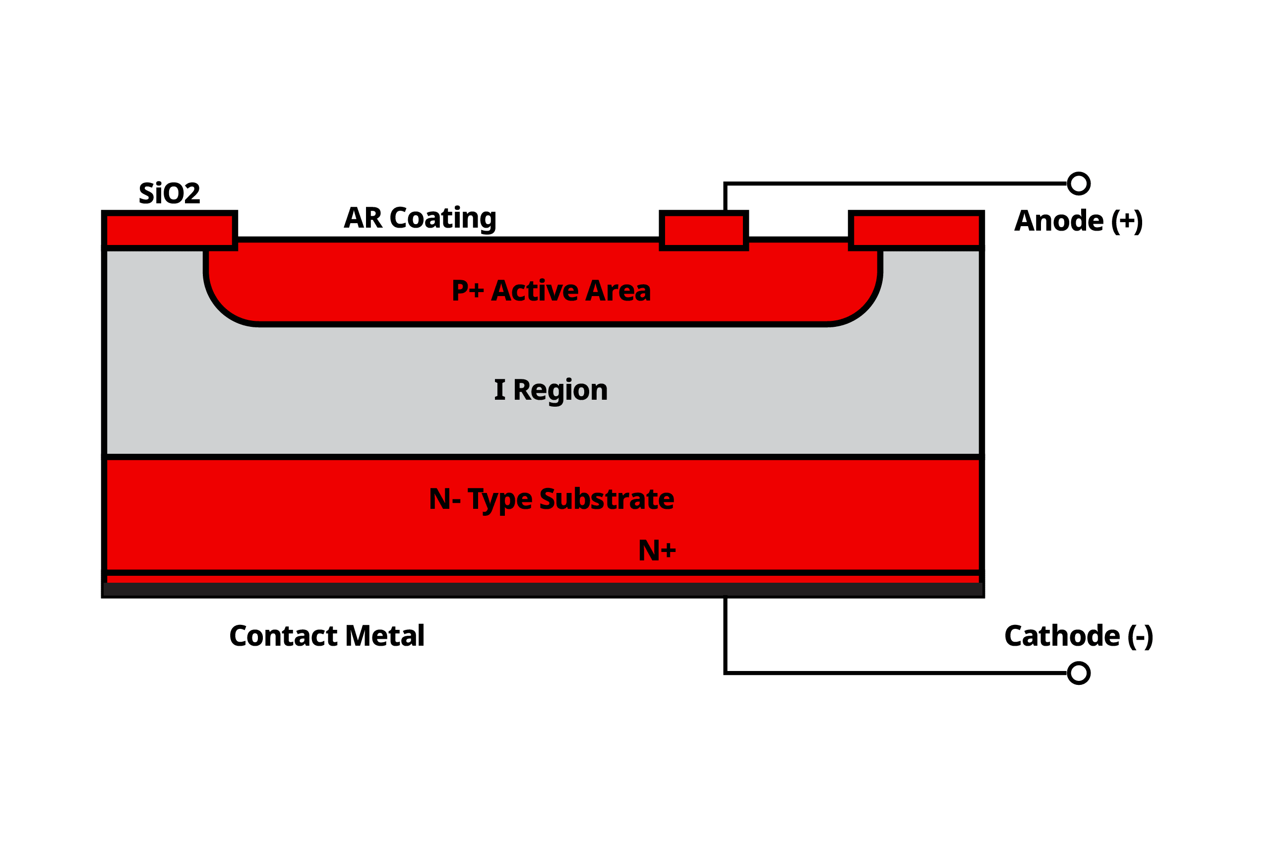
One of the most fundamental and important parts of a photodiode is the p-n junction. This is a space between two layers of semiconductor material, the p-type layer has a high number of holes while the n-type layer is packed with electrons. Though there are several types of photodiodes, this is a consistent element of the devices’ design and is usually called the depletion layer.
When no light is detected by the device, there is very little current generated within the device (often it’s close to zero). This is known as the photodiode’s ‘dark current’ and will reduce as the sensitivity of the device increases.
When light energy is detected by the device (usually above a certain set level called the bandgap) this causes new holes and electrons to be created, generating an electrical current in the p-n junction.
In photodiodes that are reverse-biased, the holes move towards the anode and the electrons to the cathode, creating a current in the depletion region. As the brightness of light increases, so does the current in the device.
Depending on the specific requirements or design of the photodiode, the device will operate in a photovoltaic or photoconductive mode:
- Photovoltaic mode is where no external voltage is applied to the device meaning it's not biased. So when light falls on the device, electrons move towards the cathode holes to the anode, generating a current in the depletion zone
- Photoconductive mode is when a reverse-biased power source is applied to the device, increasing the depletion area, dark current and response speed of the photodiode while reducing its junction capacitance
The design and structure are the key difference between photodiodes vs phototransistors. Specifically, the main elements that differ between the two devices are:
- Phototransistors have three layers of material rather than two, creating two p-n junctions
- Photodiodes only have two terminals while phototransistors can have up to three
- Phototransistors can be used only in forward bias modes, while photodiodes can operate in reverse bias
- Phototransistors have to be connected to a power source to operate, while photodiodes do not
- Photodiodes create both current and voltage while phototransistors only produce current
This means that rather than turning light into electricity, phototransistors are used as light sensors, making them suitable for applications such as smoke detectors or remote controls.
What are Photodiodes Used for?
The main application of photodiodes is solar cells in energy production systems and detecting the brightness of a light source. However, there are other specific uses where photodiode devices can be applied, including:
- Fire and smoke detectors
- Medical devices, including ones that analyse samples and monitor blood gas
- Accurate light measurement devices
- Optical communications
- Camera controls such as the shutter and flash
Why are Photodiodes Reverse Biased?
Photodiode circuits and devices operate in both forward and reverse bias.
Forward bias occurs when a voltage is applied such that the positive terminal is connected to the p-type and the negative terminal is connected to the n-type. In photoconductive mode, the photodiode is operated in reverse bias, in the opposite direction.
The reverse bias occurs when connecting an external power source to the photodiode device, with the negative terminal on the p-type layer and the positive terminal on the n-type layer.
In reverse bias mode, when the power source is switched on and light is detected by the photodiode, electrons from the n-type layer are pulled to the positive terminal and holes from the p-type layer towards the negative terminal. This causes the depletion layer to increase, reducing the junction capacitance, but enabling more photons to be absorbed.
Forward bias allows more electrons and holes to flow across the p-n junction, while reverse bias increases the width of the depletion region, making the photodiode more sensitive to light.
This means that forward bias mode is less sensitive to light than reverse bias mode. As a result, forward bias mode is commonly used in applications where a quick response time is required. For example, light-emitting diodes (LEDs) and optical sensors.
Reverse-biased photodiodes are particularly useful for light detection and measurement as they produce a photocurrent that is directly proportional to the intensity of the incident light. It is most beneficial when used in situations where high-speed and high sensitivity are critical, such as photovoltaic cells and light sensors.
In short, the main difference between forward bias and reverse bias is that, in the former, the voltage supplied enables the free flow of current across the diode. In the latter, the supplied voltage restricts current flow.
For example, a reverse bias function can be used in a photovoltaic cell to enable the voltage and current to increase or decrease in direct proportion to the amount of light exposure. If a forward bias function was used in this case, the increase after light exposure would be exponential, meaning less control over current and voltage.
Types of Photodiodes
Though the basic design of photodiodes is the same in all types, there are some specific devices with structures that make them suitable for particular applications.
Avalanche Photodiodes
As indicated by the name of this photodiode type, the structure of these devices is designed to create a high number of charge carriers. It does this by a large power supply being directed into these devices via reverse bias. As a result, these photodiodes have a higher response level than other devices.
It also means there are some drawbacks to using these devices, such as loudness, sensitivity to temperature and a decrease in operating bandwidth. Even so, avalanche photodiodes are still used in optical link systems.
PN Photodiodes
PN photodiodes are the most basic form of the device. As such, they operate as a standard photodiode and only generate electrical current when exposed to light, with no voltage supplied. However, though they’re the first type of these devices to be created, their relatively low performance means they’re not used very often nowadays.
PIN Photodiodes
Alongside the standard p-type and n-type layers, PIN photodiodes also have an intrinsic semiconductor layer in the middle of the structure. This makes the depletion layer in these devices wider than in other photodiodes. This helps more photon energy to be captured and converted into electron-hole pairs in the depletion layer.
This means PIN photodiodes have significant bandwidth and a quick response speed compared to other devices. As such they’re often used for fibre optic network systems, X-ray and gamma-ray detection and photodetectors.
Schottky Photodiodes
In Schottky photodiodes, a metal layer such as aluminium or platinum is combined with an n-type semiconductor layer. The space between them is called the metal-semiconductor junction. The size of this space differs depending on the height of the energy barrier that’s formed in this depletion zone. Electrons have to overcome this barrier to move across the device.
If the barrier height is low, the device is termed ‘non-rectifying’. If it is high, it’s called ‘rectifying’. The former presents less resistance to electric currents while the latter’s resistance is high.
This, in combination with the ability to switch the function of this device between forward and reverse bias, means these photodiodes are useful for a range of applications. This includes quick switch, radio-frequency and power supply functions.