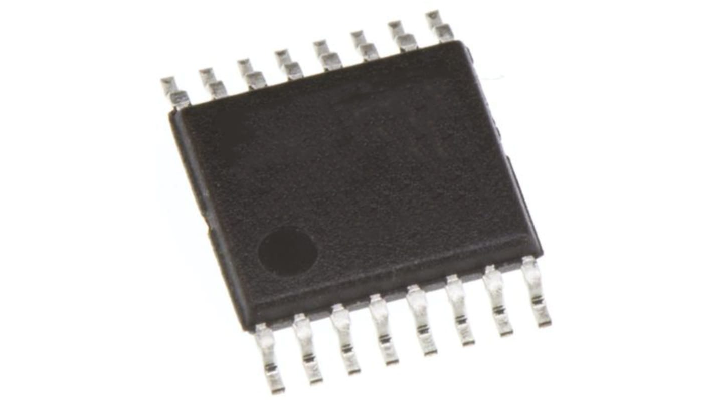
onsemi, Logic Level Translator Level Shifter 4 CMOS, TTL to CMOS, 16-Pin TSSOP
- RS Stock No.:
- 186-9328P
- Mfr. Part No.:
- MC14504BDTR2G
- Brand:
- onsemi

Bulk discount available
Subtotal 100 units (supplied on a continuous strip)*
£32.00
(exc. VAT)
£38.00
(inc. VAT)
Add 160 units to get free delivery
In Stock
- 210 unit(s) ready to ship
Need more? Click ‘Check delivery dates’ to find extra stock and lead times.
Units | Per unit |
|---|---|
| 100 - 240 | £0.32 |
| 250 - 490 | £0.277 |
| 500 - 990 | £0.244 |
| 1000 + | £0.222 |
*price indicative
- RS Stock No.:
- 186-9328P
- Mfr. Part No.:
- MC14504BDTR2G
- Brand:
- onsemi
Specifications
Technical Reference
Legislation and Compliance
Product Details
Find similar products by selecting one or more attributes.
Select all | Attribute | Value |
|---|---|---|
| Brand | onsemi | |
| Direction Type | Uni-Directional | |
| Logic Family | CMOS | |
| Product Type | Logic Level Translator | |
| Maximum Propagation Delay Time @ CL | 340ns | |
| Mount Type | Surface | |
| Package Type | TSSOP | |
| Number of Elements per Chip | 4 | |
| Pin Count | 16 | |
| Output Type | TTL | |
| Logic Function | Level Shifter | |
| Maximum Low Level Output Current | -10mA | |
| Minimum Supply Voltage | 3V | |
| Maximum High Level Output Current | 10mA | |
| Maximum Supply Voltage | 18V | |
| Translation | CMOS, TTL to CMOS | |
| Minimum Operating Temperature | -55°C | |
| Maximum Operating Temperature | 125°C | |
| Series | MC14504 | |
| Length | 5.1mm | |
| Height | 1.05mm | |
| Standards/Approvals | No | |
| Width | 4.5 mm | |
| Automotive Standard | AEC-Q100 | |
| Select all | ||
|---|---|---|
Brand onsemi | ||
Direction Type Uni-Directional | ||
Logic Family CMOS | ||
Product Type Logic Level Translator | ||
Maximum Propagation Delay Time @ CL 340ns | ||
Mount Type Surface | ||
Package Type TSSOP | ||
Number of Elements per Chip 4 | ||
Pin Count 16 | ||
Output Type TTL | ||
Logic Function Level Shifter | ||
Maximum Low Level Output Current -10mA | ||
Minimum Supply Voltage 3V | ||
Maximum High Level Output Current 10mA | ||
Maximum Supply Voltage 18V | ||
Translation CMOS, TTL to CMOS | ||
Minimum Operating Temperature -55°C | ||
Maximum Operating Temperature 125°C | ||
Series MC14504 | ||
Length 5.1mm | ||
Height 1.05mm | ||
Standards/Approvals No | ||
Width 4.5 mm | ||
Automotive Standard AEC-Q100 | ||
- COO (Country of Origin):
- CN
The MC14504B is a hex non-inverting level shifter using CMOS technology. The level shifter will shift a TTL signal to CMOS logic levels for any CMOS supply voltage between 5 and 15 volts. A control input also allows interface from CMOS to CMOS at one logic level to another logic level: Either up or down level translating is accomplished by selection of power supply levels VDD and VCC. The VCC level sets the input signal levels while VDD selects the output voltage levels.
UP Translates from a Low to a High Voltage or DOWN Translates from a High to a Low Voltage
Input Threshold Can Be Shifted for TTL Compatibility
No Sequencing Required on Power Supplies or Inputs for Power Up or Power Down
3 to 18 Vdc Operation for VDD and VCC
Diode Protected Inputs to VSS
Capable of Driving Two Low-Power TTL Loads or One Low-Power Schottky TTL Load Over the Rated Temperature Range
Pb-Free Packages are Available