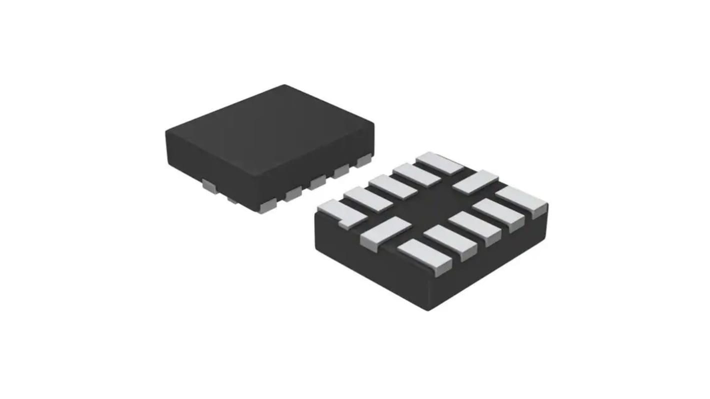
onsemi NLSV4T244MUTAG, Voltage Level Shifter Voltage Level Translator 2, 12-Pin UQFN
- RS Stock No.:
- 186-7339
- Mfr. Part No.:
- NLSV4T244MUTAG
- Brand:
- onsemi

Unavailable
RS will no longer stock this product.
- RS Stock No.:
- 186-7339
- Mfr. Part No.:
- NLSV4T244MUTAG
- Brand:
- onsemi
Specifications
Technical Reference
Legislation and Compliance
Product Details
Find similar products by selecting one or more attributes.
Select all | Attribute | Value |
|---|---|---|
| Brand | onsemi | |
| Mounting Type | Surface Mount | |
| Number of Elements per Chip | 2 | |
| Package Type | UQFN | |
| Output Type | 3 State | |
| Pin Count | 12 | |
| Dimensions | 1.7 x 2 x 0.5mm | |
| Logic Function | Voltage Level Translator | |
| Maximum Low Level Output Current | 24mA | |
| Maximum High Level Output Current | -24mA | |
| Maximum Operating Supply Voltage | 0.9 to 4.5 V | |
| Maximum Operating Temperature | +105 °C | |
| Minimum Operating Supply Voltage | 0.9 V | |
| Automotive Standard | AEC-Q100 | |
| Minimum Operating Temperature | -40 °C | |
| Select all | ||
|---|---|---|
Brand onsemi | ||
Mounting Type Surface Mount | ||
Number of Elements per Chip 2 | ||
Package Type UQFN | ||
Output Type 3 State | ||
Pin Count 12 | ||
Dimensions 1.7 x 2 x 0.5mm | ||
Logic Function Voltage Level Translator | ||
Maximum Low Level Output Current 24mA | ||
Maximum High Level Output Current -24mA | ||
Maximum Operating Supply Voltage 0.9 to 4.5 V | ||
Maximum Operating Temperature +105 °C | ||
Minimum Operating Supply Voltage 0.9 V | ||
Automotive Standard AEC-Q100 | ||
Minimum Operating Temperature -40 °C | ||
The NLSV4T244 is a 4 bit configurable dual supply voltage level translator. The input An and output Bn ports are designed to track two different power supply rails, VCCA and VCCB respectively. Both supply rails are configurable from 0.9 V to 4.5 V allowing universal low voltage translation from the input An to the output Bn port
VCCA and VCCB Operating Range: 0.9 V to 4.5 V
High-Speed w/ Balanced Propagation Delay
Inputs and Outputs have OVT Protection to 4.5 V
Non-preferential VCCA and VCCB Sequencing
Outputs at 3-State until Active VCC is Reached
Power-Off Protection
Outputs Switch to 3-State with VCCB at GND
Ultra-Small Packaging: 1.7 mm x 2.0 mm UQFN12
This is a Pb-Free Device
Benefits
Wide operating range
Allows for use with new faster processors
Higher reliability
Ease of design and re-use
Lower power in Tri-State
Higher Reliability
Lower power consumption
Lower PCB space required
Applications
Mobile Phones, PDAs, Other Portable Devices