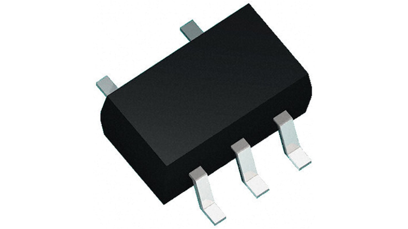
onsemi NLVSV1T34DFT2G, Logic Level Translator Voltage Level Translator, 5-Pin SC-88A
- RS Stock No.:
- 172-3308
- Mfr. Part No.:
- NLVSV1T34DFT2G
- Brand:
- onsemi

Currently unavailable
We don't know if this item will be back in stock, RS intend to remove it from our range soon.
- RS Stock No.:
- 172-3308
- Mfr. Part No.:
- NLVSV1T34DFT2G
- Brand:
- onsemi
Specifications
Technical Reference
Legislation and Compliance
Product Details
Find similar products by selecting one or more attributes.
Select all | Attribute | Value |
|---|---|---|
| Brand | onsemi | |
| Product Type | Logic Level Translator | |
| Logic Family | NLSV | |
| Mount Type | Surface Mount | |
| Package Type | SC-88A | |
| Pin Count | 5 | |
| Output Type | Single Ended | |
| Logic Function | Voltage Level Translator | |
| Maximum Low Level Output Current | 24mA | |
| Maximum High Level Output Current | -24mA | |
| Minimum Operating Temperature | -40°C | |
| Maximum Operating Temperature | 85°C | |
| Length | 2.2mm | |
| Height | 1mm | |
| Automotive Standard | AEC-Q100 | |
| Select all | ||
|---|---|---|
Brand onsemi | ||
Product Type Logic Level Translator | ||
Logic Family NLSV | ||
Mount Type Surface Mount | ||
Package Type SC-88A | ||
Pin Count 5 | ||
Output Type Single Ended | ||
Logic Function Voltage Level Translator | ||
Maximum Low Level Output Current 24mA | ||
Maximum High Level Output Current -24mA | ||
Minimum Operating Temperature -40°C | ||
Maximum Operating Temperature 85°C | ||
Length 2.2mm | ||
Height 1mm | ||
Automotive Standard AEC-Q100 | ||
The NLSV1T34 is a 1-bit configurable dual supply voltage level translator. The input An and output Bn ports are designed to track two different power supply rails, VCCA and VCCB respectively. Both supply rails are configurable from 0.9 V to 4.5 V allowing universal low voltage translation from the input An to the output Bn port.
Wide VCCA and VCCB Operating Range: 0.9 V to 4.5 V
High-Speed w/ Balanced Propagation Delay
Inputs and Outputs have OVT Protection to 4.5 V
Non-preferential VCCA and VCCB Sequencing
Power-Off Protection
UltraSmall Packaging: 1.45 mm x 1.0 mm ULLGA6 2.0 mm x 2.1 mm SC88A 1.2 mm x 1.0 mm UDFN6 1.45 mm x 1.0 mm UDFN6
This is a Pb and Halide Free Device
Applications
Mobile Phones, PDAs, Other Portable Devices
