Infineon SRAM Memory Chip, CY7C1018DV33-10VXI- 1Mbit
- RS Stock No.:
- 194-8899
- Mfr. Part No.:
- CY7C1018DV33-10VXI
- Brand:
- Infineon

Stock information currently inaccessible
- RS Stock No.:
- 194-8899
- Mfr. Part No.:
- CY7C1018DV33-10VXI
- Brand:
- Infineon
Specifications
Technical Reference
Legislation and Compliance
Product Details
Find similar products by selecting one or more attributes.
Select all | Attribute | Value |
|---|---|---|
| Brand | Infineon | |
| Memory Size | 1Mbit | |
| Organisation | 128k x 8 bit | |
| Number of Words | 128k | |
| Number of Bits per Word | 8bit | |
| Maximum Random Access Time | 10ns | |
| Address Bus Width | 8bit | |
| Clock Frequency | 1MHz | |
| Timing Type | Asynchronous | |
| Mounting Type | Surface Mount | |
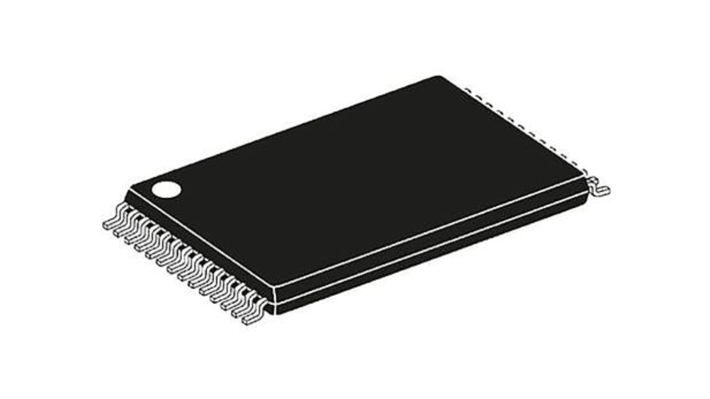
| Package Type | SOJ | |
| Pin Count | 32 | |
| Dimensions | 0.83 x 0.405 x 0.12in | |
| Maximum Operating Supply Voltage | 3.3 V | |
| Height | 3.05mm | |
| Width | 10.29mm | |
| Maximum Operating Temperature | +85 °C | |
| Minimum Operating Temperature | -40 °C | |
| Length | 21.08mm | |
| Select all | ||
|---|---|---|
Brand Infineon | ||
Memory Size 1Mbit | ||
Organisation 128k x 8 bit | ||
Number of Words 128k | ||
Number of Bits per Word 8bit | ||
Maximum Random Access Time 10ns | ||
Address Bus Width 8bit | ||
Clock Frequency 1MHz | ||
Timing Type Asynchronous | ||
Mounting Type Surface Mount | ||
Package Type SOJ | ||
Pin Count 32 | ||
Dimensions 0.83 x 0.405 x 0.12in | ||
Maximum Operating Supply Voltage 3.3 V | ||
Height 3.05mm | ||
Width 10.29mm | ||
Maximum Operating Temperature +85 °C | ||
Minimum Operating Temperature -40 °C | ||
Length 21.08mm | ||
Easy memory expansion is provided by an active LOW Chip Enable (CE), an active LOW Output Enable (OE), and three-state drivers. This device has an automatic power-down feature that significantly reduces power consumption when deselected. Writing to the device is accomplished by taking Chip Enable (CE) and Write Enable (WE) inputs LOW. Data on the eight I/O pins (I/O0 through I/O7) is then written into the location specified on the address pins (A0 through A16). Reading from the device is accomplished by taking Chip Enable (CE) and Output Enable (OE) LOW while forcing Write Enable (WE) HIGH. Under these conditions, the contents of the memory location specified by the address pins will appear on the I/O pins. The eight input/output pins (I/O0 through I/O7) are placed in a high-impedance state when the device is deselected (CE HIGH), the outputs are disabled (OE HIGH), or during a write operation (CE LOW, and WE LOW). The CY7C1018DV33/CY7C1019DV33 are available in Pb-free 32-pin 400-Mil wide Molded SOJ, 32-pin TSOP II and 48-ball VFBGA packages.
Related links
- Infineon SRAM Memory Chip, CY7C1018DV33-10VXI- 1Mbit
- Infineon SRAM Memory Chip, CY7C1021DV33-10VXIT- 1Mbit
- Infineon SRAM Memory Chip, CY7C1021D-10VXIT- 1Mbit
- Infineon SRAM, CY7C1019DV33-10VXI- 1Mbit
- Infineon SRAM Memory Chip, CY7C1049G30-10VXI- 4Mbit
- Cypress Semiconductor SRAM Memory Chip, CY62128EV30LL-45ZXI- 1Mbit
- ISSI SRAM, IS61C1024AL-12JLI- 1Mbit
- SRAM