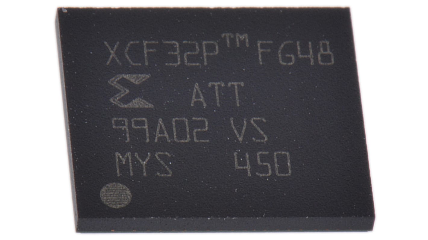
Xilinx XCF32PFSG48C, Configuration Memory 48-Pin TFBGA
- RS Stock No.:
- 173-2096
- Mfr. Part No.:
- XCF32PFSG48C
- Brand:
- Xilinx

Discontinued
- RS Stock No.:
- 173-2096
- Mfr. Part No.:
- XCF32PFSG48C
- Brand:
- Xilinx
Specifications
Technical Reference
Legislation and Compliance
Product Details
Find similar products by selecting one or more attributes.
Select all | Attribute | Value |
|---|---|---|
| Brand | Xilinx | |
| Mounting Type | Surface Mount | |
| Package Type | TFBGA | |
| Pin Count | 48 | |
| Dimensions | 9 x 8 x 0.86mm | |
| Length | 9mm | |
| Width | 8mm | |
| Height | 0.86mm | |
| Maximum Operating Supply Voltage | 2 V | |
| Maximum Operating Temperature | +85 °C | |
| Minimum Operating Supply Voltage | 1.65 V | |
| Minimum Operating Temperature | -40 °C | |
| Select all | ||
|---|---|---|
Brand Xilinx | ||
Mounting Type Surface Mount | ||
Package Type TFBGA | ||
Pin Count 48 | ||
Dimensions 9 x 8 x 0.86mm | ||
Length 9mm | ||
Width 8mm | ||
Height 0.86mm | ||
Maximum Operating Supply Voltage 2 V | ||
Maximum Operating Temperature +85 °C | ||
Minimum Operating Supply Voltage 1.65 V | ||
Minimum Operating Temperature -40 °C | ||
XCFxx Configuration Flash Memory
The XCFxx series of Flash EPROMs provide an easy-to-use, cost-effective and reprogrammable method for storing large Xilinx FPGA configuration bitstreams.
In-System Programmable Flash memory devices for configuration of Xilinx FPGAs
IEEE Standard 1149.1/1532 Boundary-Scan (JTAG) support for Programming, Prototyping, and Testing
Cascadable for storing longer or multiple bitstreams
I/O pins compatible with voltage levels ranging from +1.5V to +3.3V
IEEE Standard 1149.1/1532 Boundary-Scan (JTAG) support for Programming, Prototyping, and Testing
Cascadable for storing longer or multiple bitstreams
I/O pins compatible with voltage levels ranging from +1.5V to +3.3V