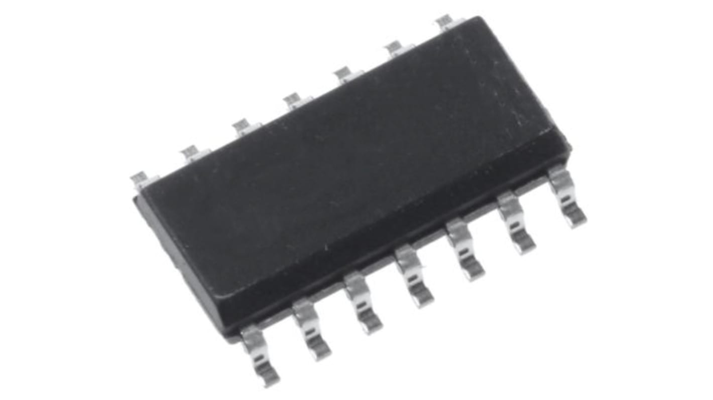
onsemi MC14016BDG Multiplexer Quad 3 to 18 V, 14-Pin SOIC
- RS Stock No.:
- 186-9745
- Mfr. Part No.:
- MC14016BDG
- Brand:
- onsemi

Subtotal (1 pack of 25 units)*
£5.55
(exc. VAT)
£6.65
(inc. VAT)
FREE delivery for orders over £50.00
In Stock
- 625 unit(s) ready to ship
Need more? Click ‘Check delivery dates’ to find extra stock and lead times.
Units | Per unit | Per Pack* |
|---|---|---|
| 25 + | £0.222 | £5.55 |
*price indicative
- RS Stock No.:
- 186-9745
- Mfr. Part No.:
- MC14016BDG
- Brand:
- onsemi
Specifications
Technical Reference
Legislation and Compliance
Product Details
Find similar products by selecting one or more attributes.
Select all | Attribute | Value |
|---|---|---|
| Brand | onsemi | |
| Pin Count | 14 | |
| Mounting Type | Surface Mount | |
| Package Type | SOIC | |
| Dimensions | 8.75 x 4 x 1.5mm | |
| Minimum Operating Temperature | -55 °C | |
| Automotive Standard | AEC-Q100 | |
| Maximum Operating Temperature | +125 °C | |
Select all | ||
|---|---|---|
Brand onsemi | ||
Pin Count 14 | ||
Mounting Type Surface Mount | ||
Package Type SOIC | ||
Dimensions 8.75 x 4 x 1.5mm | ||
Minimum Operating Temperature -55 °C | ||
Automotive Standard AEC-Q100 | ||
Maximum Operating Temperature +125 °C | ||
The MC14016B quad bilateral switch is constructed with MOS P-channel and N-channel enhancement mode devices in a single monolithic structure. Each MC14016B consists of four independent switches capable of controlling either digital or analog signals. The quad bilateral switch is used in signal gating, chopper, modulator, demodulator and CMOS logic implementation.
Diode Protection on All Inputs
Supply Voltage Range = 3.0 Vdc to 18 Vdc
Linearized Transfer Characteristics
Low Noise - 12 nV/sq. root (Cycle), f >= 1.0 kHz typical
Pin-for-Pin Replacements for CD4016B, CD4066B (Note improved transfer characteristic design causes more parasitic coupling capacitance than CD4016)
For Lower RON , Use The HC4016 High-Speed CMOS Device or The MC14066B
This Device Has Inputs and Outputs Which Do Not Have ESD Protection. Antistatic Precautions Must Be Taken.