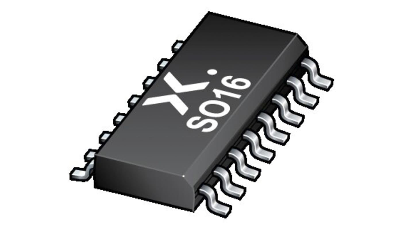
Nexperia 74HC251D,653 Multiplexer Single 8:1 5 V, 16-Pin SOIC
- RS Stock No.:
- 181-7345
- Mfr. Part No.:
- 74HC251D,653
- Brand:
- Nexperia

Subtotal (1 reel of 2500 units)*
£362.50
(exc. VAT)
£435.00
(inc. VAT)
FREE delivery for orders over £50.00
Temporarily out of stock
- Shipping from 02 January 2026
Need more? Click ‘Check delivery dates’ to find extra stock and lead times.
Units | Per unit | Per Reel* |
|---|---|---|
| 2500 + | £0.145 | £362.50 |
*price indicative
- RS Stock No.:
- 181-7345
- Mfr. Part No.:
- 74HC251D,653
- Brand:
- Nexperia
Specifications
Technical Reference
Legislation and Compliance
Product Details
Find similar products by selecting one or more attributes.
Select all | Attribute | Value |
|---|---|---|
| Brand | Nexperia | |
| Pin Count | 16 | |
| Mounting Type | Surface Mount | |
| Package Type | SO | |
| Dimensions | 10 x 4 x 1.45mm | |
| Maximum Operating Temperature | +125 °C | |
| Minimum Operating Temperature | -40 °C | |
Select all | ||
|---|---|---|
Brand Nexperia | ||
Pin Count 16 | ||
Mounting Type Surface Mount | ||
Package Type SO | ||
Dimensions 10 x 4 x 1.45mm | ||
Maximum Operating Temperature +125 °C | ||
Minimum Operating Temperature -40 °C | ||
- COO (Country of Origin):
- TH
When simplifying interface buses, we make your choice simple By enabling input expansion, digital multiplexers can simplify interface buses. Our devices cover a wide range of options to suit your particular needs. They feature low propagation delay and high noise immunity, while ensuring minimal power consumption.
Mixed 5 V and 3.3 V applications
Bus width reduction
High noise immunity
Low power consumption
Wide supply voltage range
Low propagation delay
Overvoltage tolerant input options
Complementary output options
Bus width reduction
High noise immunity
Low power consumption
Wide supply voltage range
Low propagation delay
Overvoltage tolerant input options
Complementary output options
The 74HC251, 74HCT251 is an 8-bit multiplexer with eight binary inputs (I0 to I7), three select inputs (S0 to S2) and an output enable input (OE). The select inputs select one of the eight binary inputs and route it to the complementary outputs (Y and Y). A HIGH on OE causes the outputs to assume a high-impedance OFF-state. Inputs include clamp diodes that enable the use of current limiting resistors to interface inputs to voltages in excess of VCC.
Input levels:
For 74HC251: CMOS level
For 74HCT251: TTL level
Low-power dissipation
Non-inverting data path
Multiple package options
Specified from -40 °C to +85 °C and from -40 °C to +125 °C
For 74HC251: CMOS level
For 74HCT251: TTL level
Low-power dissipation
Non-inverting data path
Multiple package options
Specified from -40 °C to +85 °C and from -40 °C to +125 °C