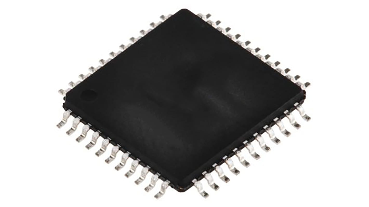
Cypress Semiconductor CY8C27543-24AXI, 8bit Microcontroller, CY8C27543, 24MHz, 16 kB Flash, 44-Pin TQFP
- RS Stock No.:
- 194-9104
- Mfr. Part No.:
- CY8C27543-24AXI
- Brand:
- Cypress Semiconductor

Unavailable
RS will no longer stock this product.
- RS Stock No.:
- 194-9104
- Mfr. Part No.:
- CY8C27543-24AXI
- Brand:
- Cypress Semiconductor
Specifications
Technical Reference
Legislation and Compliance
Product Details
Find similar products by selecting one or more attributes.
Select all | Attribute | Value |
|---|---|---|
| Brand | Cypress Semiconductor | |
| Family Name | CY8C27543 | |
| Package Type | TQFP | |
| Mounting Type | Surface Mount | |
| Pin Count | 44 | |
| Data Bus Width | 8bit | |
| Program Memory Size | 16 kB | |
| Maximum Frequency | 24MHz | |
| RAM Size | 256 B | |
| USB Channels | 1 | |
| Number of PWM Units | 2 x 8/16 bit | |
| Number of SPI Channels | 1 | |
| Number of UART Channels | 1 | |
| Typical Operating Supply Voltage | 3 → 5.25 V | |
| Number of I2C Channels | 1 | |
| Number of ADC Units | 1 | |
| ADCs | 1 x 14 bit | |
| Height | 1.4mm | |
| Width | 10mm | |
| Data Rate | 400kbit/s | |
| Program Memory Type | Flash | |
| Minimum Operating Temperature | -40 °C | |
| Dimensions | 10 x 10 x 1.4mm | |
| Maximum Operating Temperature | +85 °C | |
| Instruction Set Architecture | Harvard | |
| Pulse Width Modulation | 1 (1 x 16 bit), 1 (1 x 8 bit) | |
| Length | 10mm | |
| Select all | ||
|---|---|---|
Brand Cypress Semiconductor | ||
Family Name CY8C27543 | ||
Package Type TQFP | ||
Mounting Type Surface Mount | ||
Pin Count 44 | ||
Data Bus Width 8bit | ||
Program Memory Size 16 kB | ||
Maximum Frequency 24MHz | ||
RAM Size 256 B | ||
USB Channels 1 | ||
Number of PWM Units 2 x 8/16 bit | ||
Number of SPI Channels 1 | ||
Number of UART Channels 1 | ||
Typical Operating Supply Voltage 3 → 5.25 V | ||
Number of I2C Channels 1 | ||
Number of ADC Units 1 | ||
ADCs 1 x 14 bit | ||
Height 1.4mm | ||
Width 10mm | ||
Data Rate 400kbit/s | ||
Program Memory Type Flash | ||
Minimum Operating Temperature -40 °C | ||
Dimensions 10 x 10 x 1.4mm | ||
Maximum Operating Temperature +85 °C | ||
Instruction Set Architecture Harvard | ||
Pulse Width Modulation 1 (1 x 16 bit), 1 (1 x 8 bit) | ||
Length 10mm | ||
- COO (Country of Origin):
- TW
These devices are designed to replace multiple traditional microcontroller unit (MCU)-based system components with one, low-cost single-chip programmable device. PSoC devices include configurable blocks of analogue and digital logic, as well as programmable interconnects. This architecture lets you to create customized peripheral configurations that match the requirements of each individual application. Additionally, a fast central processing unit (CPU), flash program memory, SRAM data memory, and configurable I/O are included in a range of convenient pinouts and packages. The PSoC architecture, as illustrated in Logic Block Diagram, consists of four main areas: PSoC core, digital system, analogue system, and system resources. Configurable global busing allows all the device resources to be combined into a complete custom system. The PSoC CY8C27x43 family can have up to five I/O ports that connect to the global digital and analogue interconnects, providing access to eight digital blocks and 12 analogue blocks.