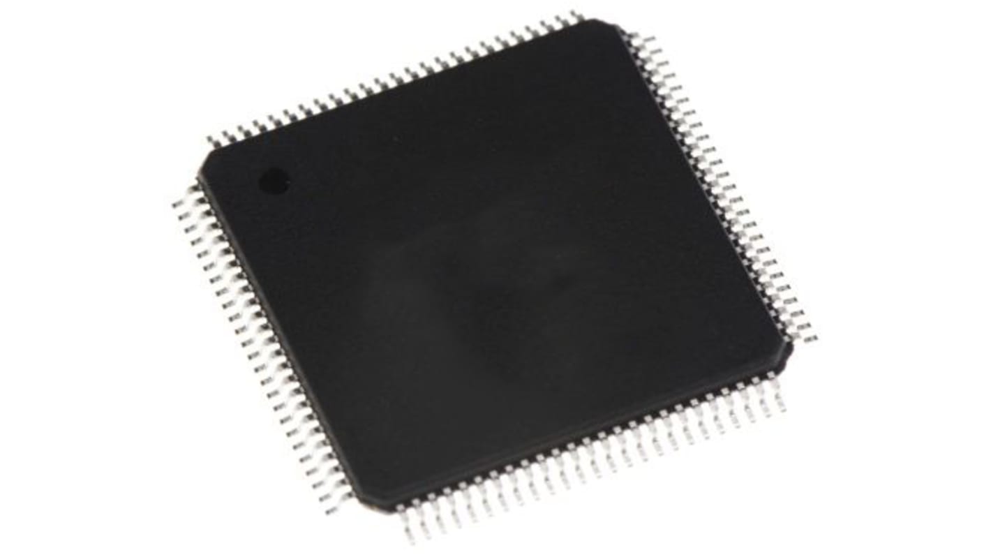
Infineon, 32bit ARM Cortex M3, CY8C58LP Microcontroller, 67MHz, 256 kB Flash, 100-Pin TQFP
- RS Stock No.:
- 188-5380
- Mfr. Part No.:
- CY8C5888AXI-LP096
- Brand:
- Infineon

Subtotal (1 tray of 90 units)*
£1,584.90
(exc. VAT)
£1,901.70
(inc. VAT)
FREE delivery for orders over £50.00
In Stock
- 540 unit(s) ready to ship
Need more? Click ‘Check delivery dates’ to find extra stock and lead times.
Units | Per unit | Per Tray* |
|---|---|---|
| 90 + | £17.61 | £1,584.90 |
*price indicative
- RS Stock No.:
- 188-5380
- Mfr. Part No.:
- CY8C5888AXI-LP096
- Brand:
- Infineon
Specifications
Technical Reference
Legislation and Compliance
Product Details
Find similar products by selecting one or more attributes.
Select all | Attribute | Value |
|---|---|---|
| Brand | Infineon | |
| Family Name | CY8C58LP | |
| Package Type | TQFP | |
| Mounting Type | Surface Mount | |
| Pin Count | 100 | |
| Device Core | ARM Cortex M3 | |
| Data Bus Width | 32bit | |
| Program Memory Size | 256 kB | |
| Maximum Frequency | 67MHz | |
| RAM Size | 64 kB | |
| USB Channels | 1 | |
| Typical Operating Supply Voltage | 1.8 → 5.5 V | |
| Number of I2C Channels | 1 | |
| Number of ADC Units | 2 | |
| Length | 14mm | |
| Program Memory Type | Flash | |
| Maximum Operating Temperature | +85 °C | |
| ADCs | 3 x 12/20 bit | |
| Minimum Operating Temperature | -40 °C | |
| Dimensions | 14 x 14 x 1.4mm | |
| Instruction Set Architecture | Thumb-2 | |
| Width | 14mm | |
| Height | 1.4mm | |
Select all | ||
|---|---|---|
Brand Infineon | ||
Family Name CY8C58LP | ||
Package Type TQFP | ||
Mounting Type Surface Mount | ||
Pin Count 100 | ||
Device Core ARM Cortex M3 | ||
Data Bus Width 32bit | ||
Program Memory Size 256 kB | ||
Maximum Frequency 67MHz | ||
RAM Size 64 kB | ||
USB Channels 1 | ||
Typical Operating Supply Voltage 1.8 → 5.5 V | ||
Number of I2C Channels 1 | ||
Number of ADC Units 2 | ||
Length 14mm | ||
Program Memory Type Flash | ||
Maximum Operating Temperature +85 °C | ||
ADCs 3 x 12/20 bit | ||
Minimum Operating Temperature -40 °C | ||
Dimensions 14 x 14 x 1.4mm | ||
Instruction Set Architecture Thumb-2 | ||
Width 14mm | ||
Height 1.4mm | ||
- COO (Country of Origin):
- US
PSoC 5LP (ARM Cortex-M3 Core), Cypress
The Cypress Semiconductor PSoC 5LP (Programmable Embedded System-on-Chip) incorporates configurable memory, microcontroller (MCU), analogue and digital peripherals all on one chip (IC). The PSoC 5LP platform architecture has a 32-bit ARM Cortex-M3 core along with direct memory access (DMA) controller and digital filter processor up to 80 MHz.
Flexible routing
Wide voltage range
Wide voltage range
Operating characteristics
Voltage range: 1.71 to 5.5 V, up to 6 power domains
Temperature range (ambient): –40 to 85 °C [1 Extended temperature parts: –40 to 105 °C
DC to 80-MHz operation
Power modes
Active mode 3.1 mA at 6 MHz, and 15.4 mA at 48 MHz
2-μA sleep mode
300-nA hibernate mode with RAM retention
Boost regulator from 0.5-V input up to 5-V output
Performance
32-bit Arm Cortex-M3 CPU, 32 interrupt inputs
24-channel direct memory access (DMA) controller
24-bit 64-tap fixed-point digital filter processor (DFB)
Memories
Up to 256 KB program flash, with cache and security features
Up to 32 KB additional flash for error correcting code (ECC)
Up to 64 KB RAM
2 KB EEPROM
Digital peripherals
Four 16-bit timer, counter, and PWM (TCPWM) blocks
I2C, 1 Mbps bus speed
USB 2.0 certified Full-Speed (FS) 12 Mbps peripheral interface (TID#10840032) using internal oscillator[2]
Full CAN 2.0b, 16 Rx, 8 Tx buffers
20 to 24 universal digital blocks (UDB), programmable to create any number of functions:
8-, 16-, 24-, and 32-bit timers, counters, and PWMs
I2C, UART, SPI, I2S, LIN 2.0 interfaces
Cyclic redundancy check (CRC)
Pseudo random sequence (PRS) generators
Quadrature decoders
Gate-level logic functions