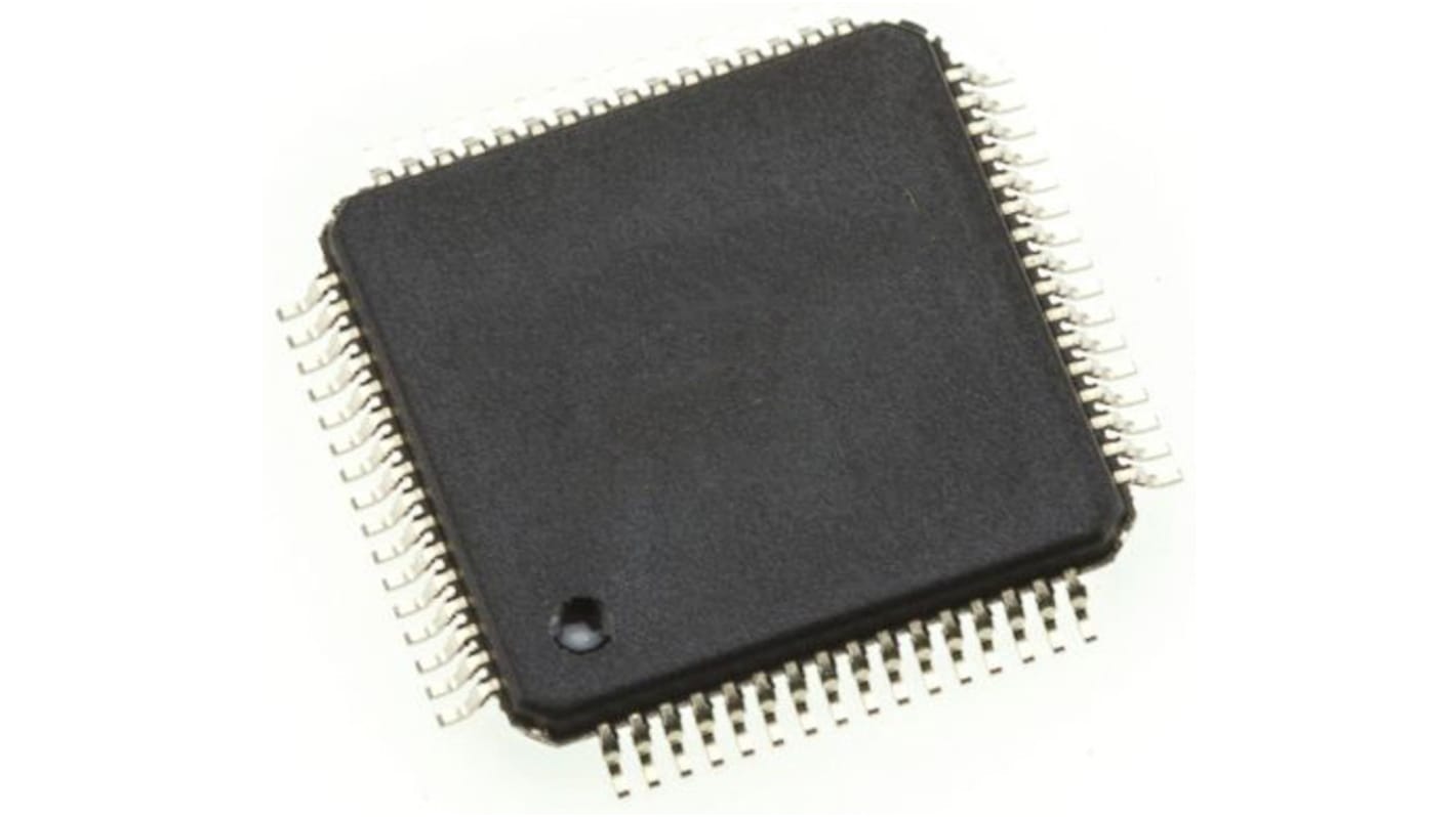
Infineon, 32bit ARM Cortex M0, CY8C4100 Microcontroller, 48MHz, 128 kB Flash, 64-Pin TQFP
- RS Stock No.:
- 176-9000
- Mfr. Part No.:
- CY8C4147AXI-S475
- Brand:
- Infineon

Subtotal (1 unit)*
£3.85
(exc. VAT)
£4.62
(inc. VAT)
FREE delivery for orders over £50.00
- 180 unit(s) ready to ship
Units | Per unit |
|---|---|
| 1 + | £3.85 |
*price indicative
- RS Stock No.:
- 176-9000
- Mfr. Part No.:
- CY8C4147AXI-S475
- Brand:
- Infineon
Select all | Attribute | Value |
|---|---|---|
| Brand | Infineon | |
| Family Name | CY8C4100 | |
| Package Type | TQFP | |
| Mounting Type | Surface Mount | |
| Pin Count | 64 | |
| Device Core | ARM Cortex M0 | |
| Data Bus Width | 32bit | |
| Program Memory Size | 128 kB | |
| Maximum Frequency | 48MHz | |
| RAM Size | 16 kB | |
| USB Channels | 0 | |
| Number of PWM Units | 1 x 16 bit | |
| Number of SPI Channels | 5 | |
| Number of I2C Channels | 5 | |
| Number of CAN Channels | 1 | |
| Number of UART Channels | 5 | |
| Number of USART Channels | 0 | |
| Typical Operating Supply Voltage | 1.8 → 5.5 V | |
| Width | 14.05mm | |
| Program Memory Type | Flash | |
| Number of PCI Channels | 0 | |
| Dimensions | 14.05 x 14.05 x 1.45mm | |
| Length | 14.05mm | |
| ADCs | 2 x 10/12 bit | |
| Maximum Number of Ethernet Channels | 0 | |
| Instruction Set Architecture | Thumb-2 | |
| Minimum Operating Temperature | -40 °C | |
| Maximum Operating Temperature | +85 °C | |
| Number of ADC Units | 1 | |
| Pulse Width Modulation | 1 (8 x 16 bit) | |
| Number of Ethernet Channels | 0 | |
| Number of LIN Channels | 0 | |
| Height | 1.45mm | |
Select all | ||
|---|---|---|
Brand Infineon | ||
Family Name CY8C4100 | ||
Package Type TQFP | ||
Mounting Type Surface Mount | ||
Pin Count 64 | ||
Device Core ARM Cortex M0 | ||
Data Bus Width 32bit | ||
Program Memory Size 128 kB | ||
Maximum Frequency 48MHz | ||
RAM Size 16 kB | ||
USB Channels 0 | ||
Number of PWM Units 1 x 16 bit | ||
Number of SPI Channels 5 | ||
Number of I2C Channels 5 | ||
Number of CAN Channels 1 | ||
Number of UART Channels 5 | ||
Number of USART Channels 0 | ||
Typical Operating Supply Voltage 1.8 → 5.5 V | ||
Width 14.05mm | ||
Program Memory Type Flash | ||
Number of PCI Channels 0 | ||
Dimensions 14.05 x 14.05 x 1.45mm | ||
Length 14.05mm | ||
ADCs 2 x 10/12 bit | ||
Maximum Number of Ethernet Channels 0 | ||
Instruction Set Architecture Thumb-2 | ||
Minimum Operating Temperature -40 °C | ||
Maximum Operating Temperature +85 °C | ||
Number of ADC Units 1 | ||
Pulse Width Modulation 1 (8 x 16 bit) | ||
Number of Ethernet Channels 0 | ||
Number of LIN Channels 0 | ||
Height 1.45mm | ||
Four programmable logic blocks called universal digital blocks, (UDBs), each with eight macrocells and data path
Cypress-provided peripheral component library, user-defined state machines, and Verilog input
Power Management:
Active mode: 1.7 mA at 3-MHz flash program execution
Deep Sleep mode: 1.5 μA with watch crystal oscillator