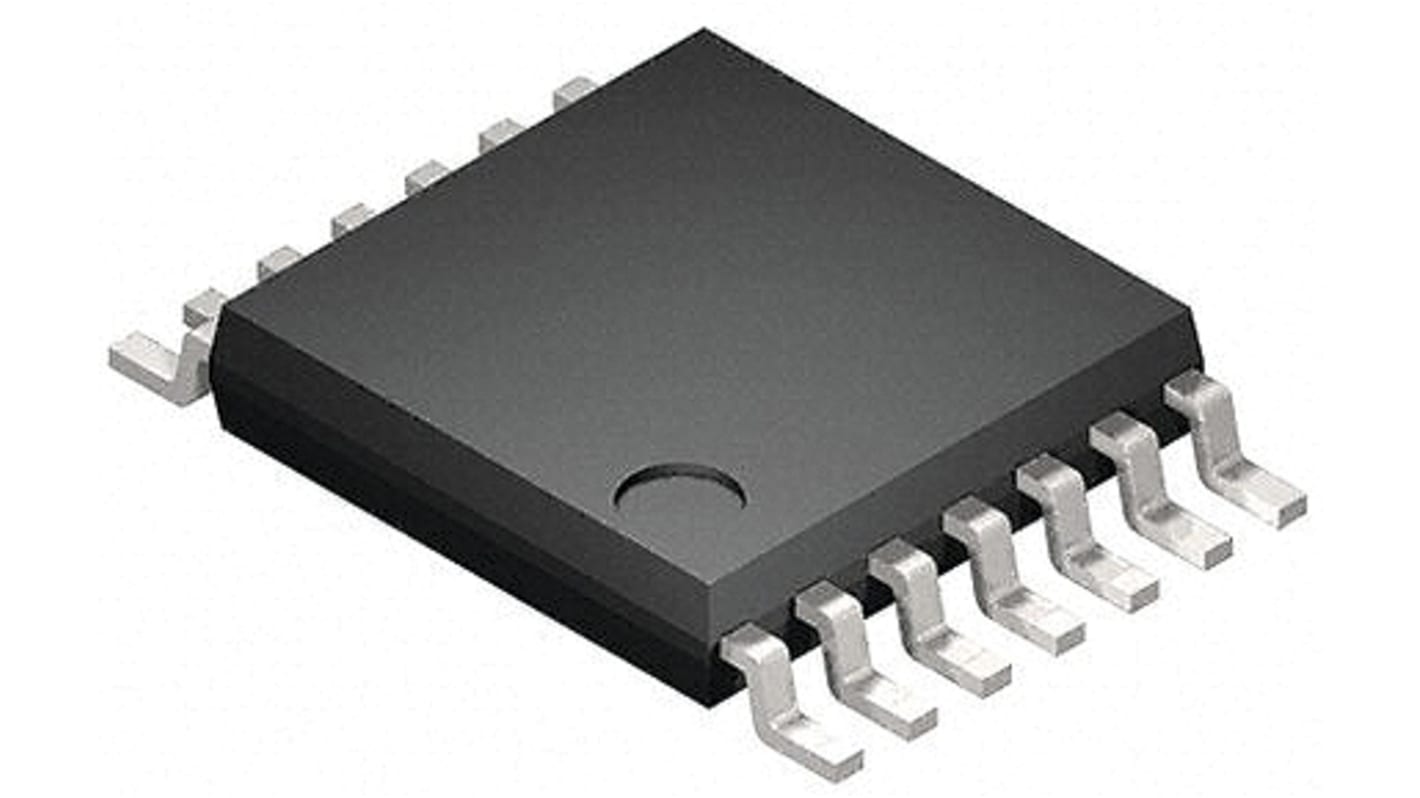
Toshiba 74VHC08FT, 4 2-Input AND Logic Gate, 14-Pin TSSOP
- RS Stock No.:
- 171-3594
- Mfr. Part No.:
- 74VHC08FT
- Brand:
- Toshiba

Subtotal (1 pack of 50 units)*
£10.70
(exc. VAT)
£12.85
(inc. VAT)
FREE delivery for orders over £60.00
- 7,950 unit(s) ready to ship
Units | Per unit | Per Pack* |
|---|---|---|
| 50 + | £0.214 | £10.70 |
*price indicative
- RS Stock No.:
- 171-3594
- Mfr. Part No.:
- 74VHC08FT
- Brand:
- Toshiba
Select all | Attribute | Value |
|---|---|---|
| Brand | Toshiba | |
| Logic Function | AND | |
| Product Type | Logic Gate | |
| Mount Type | Surface | |
| Number of Elements | 4 | |
| Number of Inputs per Gate | 2 | |
| Schmitt Trigger Input | No | |
| Package Type | TSSOP | |
| Pin Count | 14 | |
| Logic Family | 74VHC | |
| Input Type | CMOS, TTL | |
| Maximum Propagation Delay Time @ CL | 10ns | |
| Minimum Operating Temperature | -40°C | |
| Maximum High Level Output Current | -8mA | |
| Maximum Operating Temperature | 125°C | |
| Length | 5mm | |
| Minimum Supply Voltage | 2V | |
| Maximum Supply Voltage | 5.5V | |
| Series | 74HC | |
| Standards/Approvals | No | |
| Height | 1mm | |
| Maximum Low Level Output Current | 8mA | |
| Output Type | CMOS, Buffer | |
| Automotive Standard | AEC-Q100 | |
| Select all | ||
|---|---|---|
Brand Toshiba | ||
Logic Function AND | ||
Product Type Logic Gate | ||
Mount Type Surface | ||
Number of Elements 4 | ||
Number of Inputs per Gate 2 | ||
Schmitt Trigger Input No | ||
Package Type TSSOP | ||
Pin Count 14 | ||
Logic Family 74VHC | ||
Input Type CMOS, TTL | ||
Maximum Propagation Delay Time @ CL 10ns | ||
Minimum Operating Temperature -40°C | ||
Maximum High Level Output Current -8mA | ||
Maximum Operating Temperature 125°C | ||
Length 5mm | ||
Minimum Supply Voltage 2V | ||
Maximum Supply Voltage 5.5V | ||
Series 74HC | ||
Standards/Approvals No | ||
Height 1mm | ||
Maximum Low Level Output Current 8mA | ||
Output Type CMOS, Buffer | ||
Automotive Standard AEC-Q100 | ||
