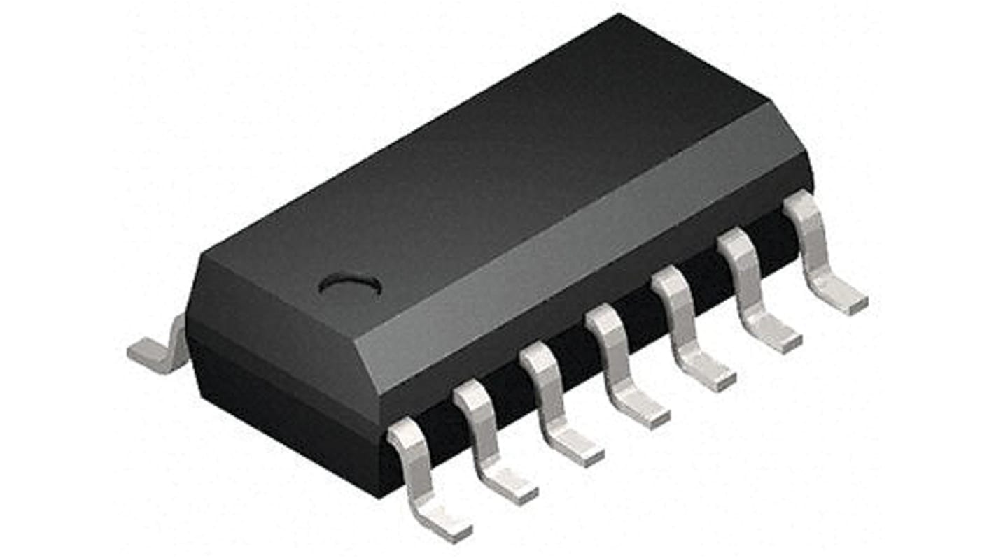
Toshiba 74HC21D, 2 4-Input AND Logic Gate, 14-Pin SOIC
- RS Stock No.:
- 171-3385
- Mfr. Part No.:
- 74HC21D
- Brand:
- Toshiba

Currently unavailable
We don't know if this item will be back in stock, RS intend to remove it from our range soon.
- RS Stock No.:
- 171-3385
- Mfr. Part No.:
- 74HC21D
- Brand:
- Toshiba
Specifications
Technical Reference
Legislation and Compliance
Product Details
Find similar products by selecting one or more attributes.
Select all | Attribute | Value |
|---|---|---|
| Brand | Toshiba | |
| Product Type | Logic Gate | |
| Logic Function | AND | |
| Mount Type | Surface | |
| Number of Elements | 2 | |
| Number of Inputs per Gate | 4 | |
| Schmitt Trigger Input | No | |
| Package Type | SOIC | |
| Pin Count | 14 | |
| Logic Family | 74HC | |
| Input Type | CMOS | |
| Maximum High Level Output Current | -5.2mA | |
| Minimum Operating Temperature | -40°C | |
| Maximum Propagation Delay Time @ CL | 25ns | |
| Maximum Operating Temperature | 85°C | |
| Maximum Supply Voltage | 6V | |
| Series | 74HC | |
| Width | 3.9mm | |
| Standards/Approvals | No | |
| Length | 8.95mm | |
| Height | 1.38mm | |
| Minimum Supply Voltage | 2V | |
| Maximum Low Level Output Current | 5.2mA | |
| Output Type | Buffer, CMOS | |
| Automotive Standard | No | |
| Select all | ||
|---|---|---|
Brand Toshiba | ||
Product Type Logic Gate | ||
Logic Function AND | ||
Mount Type Surface | ||
Number of Elements 2 | ||
Number of Inputs per Gate 4 | ||
Schmitt Trigger Input No | ||
Package Type SOIC | ||
Pin Count 14 | ||
Logic Family 74HC | ||
Input Type CMOS | ||
Maximum High Level Output Current -5.2mA | ||
Minimum Operating Temperature -40°C | ||
Maximum Propagation Delay Time @ CL 25ns | ||
Maximum Operating Temperature 85°C | ||
Maximum Supply Voltage 6V | ||
Series 74HC | ||
Width 3.9mm | ||
Standards/Approvals No | ||
Length 8.95mm | ||
Height 1.38mm | ||
Minimum Supply Voltage 2V | ||
Maximum Low Level Output Current 5.2mA | ||
Output Type Buffer, CMOS | ||
Automotive Standard No | ||
The 74HC21D is a high speed CMOS 4-INPUT AND GATE fabricated with silicon gate C2MOS technology. It achieves the high speed operation similar to equivalent LSTTL while maintaining the CMOS low power dissipation. The internal circuit is composed of 4 stages including buffer an output, which provide high noise immunity and stable output. All inputs are equipped with protection circuits against static discharge or transient excess voltage
High speed: tpd = 10 ns (typ.) at VCC = 5 V
Low power dissipation: ICC = 1.0 μA (max) Ta = 25
Balanced propagation delays: tPLH ≈ tPHL
Wide operating voltage range: VCC(opr) = 2.0 to 6.0 V