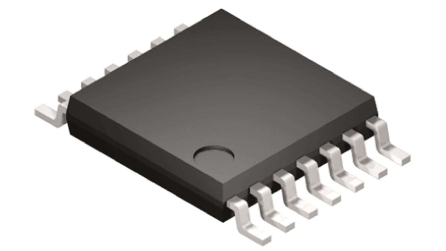
Nexperia 74LVC125APW,112, 4 4-Input Buffer & Line Driver Logic Gate, 14-Pin TSSOP
- RS Stock No.:
- 124-2270
- Mfr. Part No.:
- 74LVC125APW,112
- Brand:
- Nexperia

Subtotal (1 tube of 96 units)*
£7.392
(exc. VAT)
£8.832
(inc. VAT)
FREE delivery for orders over £60.00
- 7,872 unit(s) shipping from 18 May 2026
Units | Per unit | Per Tube* |
|---|---|---|
| 96 + | £0.077 | £7.39 |
*price indicative
- RS Stock No.:
- 124-2270
- Mfr. Part No.:
- 74LVC125APW,112
- Brand:
- Nexperia
Select all | Attribute | Value |
|---|---|---|
| Brand | Nexperia | |
| Product Type | Logic Gate | |
| Logic Function | Buffer & Line Driver | |
| Mount Type | Surface | |
| Number of Elements | 4 | |
| Number of Inputs per Gate | 4 | |
| Schmitt Trigger Input | No | |
| Package Type | TSSOP | |
| Pin Count | 14 | |
| Logic Family | LVC | |
| Input Type | Single Ended | |
| Maximum Propagation Delay Time @ CL | 6ns | |
| Maximum High Level Output Current | -24mA | |
| Minimum Operating Temperature | -40°C | |
| Maximum Operating Temperature | 125°C | |
| Length | 5.1mm | |
| Maximum Supply Voltage | 3.6V | |
| Standards/Approvals | No | |
| Minimum Supply Voltage | 1.2V | |
| Height | 0.95mm | |
| Maximum Low Level Output Current | 24mA | |
| Automotive Standard | No | |
| Output Type | 3 State | |
| Select all | ||
|---|---|---|
Brand Nexperia | ||
Product Type Logic Gate | ||
Logic Function Buffer & Line Driver | ||
Mount Type Surface | ||
Number of Elements 4 | ||
Number of Inputs per Gate 4 | ||
Schmitt Trigger Input No | ||
Package Type TSSOP | ||
Pin Count 14 | ||
Logic Family LVC | ||
Input Type Single Ended | ||
Maximum Propagation Delay Time @ CL 6ns | ||
Maximum High Level Output Current -24mA | ||
Minimum Operating Temperature -40°C | ||
Maximum Operating Temperature 125°C | ||
Length 5.1mm | ||
Maximum Supply Voltage 3.6V | ||
Standards/Approvals No | ||
Minimum Supply Voltage 1.2V | ||
Height 0.95mm | ||
Maximum Low Level Output Current 24mA | ||
Automotive Standard No | ||
Output Type 3 State | ||
- COO (Country of Origin):
- TH
Related links
- Nexperia 74LVC125APW 4 4-Input Buffer & Line Driver Schmitt Trigger Input Logic Gate, 14-Pin TSSOP
- Nexperia 74HC125D 4 4-Input Buffer & Line Driver Logic Gate, 14-Pin SO
- Nexperia 74HC125D 4 4-Input Buffer & Line Driver Logic Gate, 14-Pin SOIC
- Nexperia 74HC02PW 4 2-Input NOR Logic Gate, 14-Pin TSSOP
- Nexperia 74LV08D 4 2-Input AND Logic Gate, 14-Pin SOIC
- onsemi 74LCX07MTCX 14-Pin TSSOP
- onsemi 14-Pin TSSOP
- Nexperia 74LVC08APW 14-Pin TSSOP
