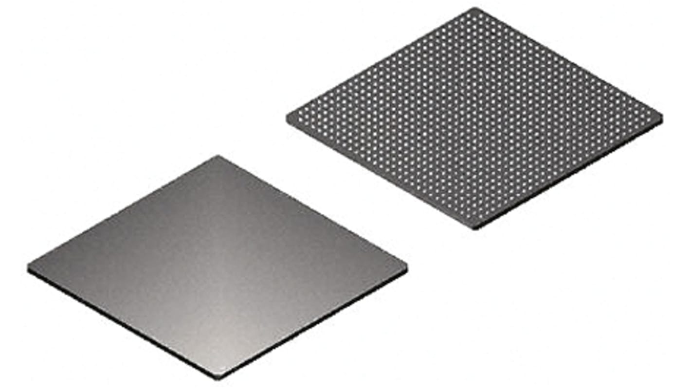
Altera FPGA 5AGXMA1D4F31I5N, Arria V 75000 Cells, 75k Gates, 8463kbit, 75000 Blocks, 896-Pin FBGA
- RS Stock No.:
- 830-3600
- Mfr. Part No.:
- 5AGXMA1D4F31I5N
- Brand:
- Altera

Bulk discount available
Subtotal (1 unit)*
£357.33
(exc. VAT)
£428.80
(inc. VAT)
Stock information currently inaccessible - Please check back later
Units | Per unit |
|---|---|
| 1 - 4 | £357.33 |
| 5 - 9 | £320.89 |
| 10 - 24 | £312.66 |
| 25 + | £304.85 |
*price indicative
- RS Stock No.:
- 830-3600
- Mfr. Part No.:
- 5AGXMA1D4F31I5N
- Brand:
- Altera
Specifications
Technical Reference
Legislation and Compliance
Find similar products by selecting one or more attributes.
Select all | Attribute | Value |
|---|---|---|
| Brand | Altera | |
| Family Name | Arria V | |
| Number of Logic Gates | 75k | |
| Number of Logic Cells | 75000 | |
| Number of Logic Units | 75000 | |
| Dedicated DSP | Yes | |
| Number of Registers | 113208 | |
| Number of Multipliers | 240 (27 x 27), 480 (18 x 18), 720 (9 x 9) | |
| Mounting Type | Surface Mount | |
| Package Type | FBGA | |
| Pin Count | 896 | |
| Number of RAM Bits | 8463kbit | |
| Dimensions | 31 x 31 x 2.1mm | |
| Height | 2.1mm | |
| Length | 31mm | |
| Maximum Operating Supply Voltage | 1.13 V | |
| Width | 31mm | |
| Minimum Operating Temperature | -40 °C | |
| Minimum Operating Supply Voltage | 1.07 V | |
| Maximum Operating Temperature | +100 °C | |
| Select all | ||
|---|---|---|
Brand Altera | ||
Family Name Arria V | ||
Number of Logic Gates 75k | ||
Number of Logic Cells 75000 | ||
Number of Logic Units 75000 | ||
Dedicated DSP Yes | ||
Number of Registers 113208 | ||
Number of Multipliers 240 (27 x 27), 480 (18 x 18), 720 (9 x 9) | ||
Mounting Type Surface Mount | ||
Package Type FBGA | ||
Pin Count 896 | ||
Number of RAM Bits 8463kbit | ||
Dimensions 31 x 31 x 2.1mm | ||
Height 2.1mm | ||
Length 31mm | ||
Maximum Operating Supply Voltage 1.13 V | ||
Width 31mm | ||
Minimum Operating Temperature -40 °C | ||
Minimum Operating Supply Voltage 1.07 V | ||
Maximum Operating Temperature +100 °C | ||