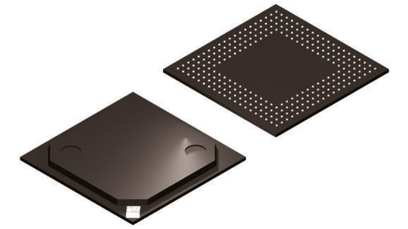
Altera FPGA 5CEBA4F17C8N 5CEBA4 49000 Cells, 49000 Gates, 3464192 bit 18480 Blocks, 256-Pin FBGA
- RS Stock No.:
- 830-3565P
- Mfr. Part No.:
- 5CEBA4F17C8N
- Brand:
- Altera

Subtotal 1 unit (supplied in a tray)*
£58.08
(exc. VAT)
£69.70
(inc. VAT)
FREE delivery for orders over £50.00
Temporarily out of stock
- Shipping from 06 July 2026
Need more? Click ‘Check delivery dates’ to find extra stock and lead times.
Units | Per unit |
|---|---|
| 1 + | £58.08 |
*price indicative
- RS Stock No.:
- 830-3565P
- Mfr. Part No.:
- 5CEBA4F17C8N
- Brand:
- Altera
Specifications
Technical Reference
Legislation and Compliance
Product Details
Find similar products by selecting one or more attributes.
Select all | Attribute | Value |
|---|---|---|
| Brand | Altera | |
| Series | 5CEBA4 | |
| Product Type | FPGA | |
| Number of Logic Gates | 49000 | |
| Number of Logic Cells | 49000 | |
| Number of Logic Units | 18480 | |
| Number of Registers | 73920 | |
| Number of Multipliers | 132 | |
| Mount Type | Surface | |
| Minimum Supply Voltage | 1.07V | |
| Package Type | FBGA | |
| Maximum Supply Voltage | 1.13V | |
| Pin Count | 256 | |
| Number of RAM Bits | 3464192bit | |
| Minimum Operating Temperature | 0°C | |
| Number of I/Os | 176 | |
| Maximum Operating Temperature | 85°C | |
| Width | 17 mm | |
| Standards/Approvals | No | |
| Length | 17mm | |
| Automotive Standard | No | |
| Select all | ||
|---|---|---|
Brand Altera | ||
Series 5CEBA4 | ||
Product Type FPGA | ||
Number of Logic Gates 49000 | ||
Number of Logic Cells 49000 | ||
Number of Logic Units 18480 | ||
Number of Registers 73920 | ||
Number of Multipliers 132 | ||
Mount Type Surface | ||
Minimum Supply Voltage 1.07V | ||
Package Type FBGA | ||
Maximum Supply Voltage 1.13V | ||
Pin Count 256 | ||
Number of RAM Bits 3464192bit | ||
Minimum Operating Temperature 0°C | ||
Number of I/Os 176 | ||
Maximum Operating Temperature 85°C | ||
Width 17 mm | ||
Standards/Approvals No | ||
Length 17mm | ||
Automotive Standard No | ||
Cyclone FPGA, Altera
An FPGA is a semiconductor device consisting of a Matrix of Configurable Logic Blocks (CLBs) connected through programmable interconnects. The user determines these interconnections by programming SRAM. A CLB can be simple (AND, OR gates, etc) or complex (a Block of RAM). The FPGA allows changes to be MADE to a design even after the device is soldered into a PCB.