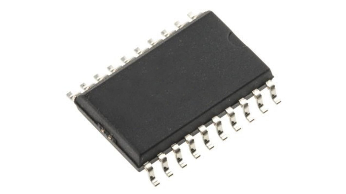
onsemi MC74AC273DWG D Type Flip Flop IC, 20-Pin SOIC
- RS Stock No.:
- 186-9263P
- Mfr. Part No.:
- MC74AC273DWG
- Brand:
- onsemi

Subtotal 25 units (supplied in a tube)*
£15.925
(exc. VAT)
£19.10
(inc. VAT)
FREE delivery for orders over £50.00
In Stock
- Plus 25 unit(s) shipping from 20 October 2025
Need more? Click ‘Check delivery dates’ to find extra stock and lead times.
Units | Per unit |
|---|---|
| 25 + | £0.637 |
*price indicative
- RS Stock No.:
- 186-9263P
- Mfr. Part No.:
- MC74AC273DWG
- Brand:
- onsemi
Specifications
Technical Reference
Legislation and Compliance
Product Details
Find similar products by selecting one or more attributes.
Select all | Attribute | Value |
|---|---|---|
| Brand | onsemi | |
| Logic Family | AC | |
| Logic Function | D Type | |
| Input Type | TTL | |
| Mounting Type | Surface Mount | |
| Package Type | SOIC | |
| Pin Count | 20 | |
| Set/Reset | Master Reset | |
| Number of Elements per Chip | 1 | |
| Maximum Propagation Delay Time @ Maximum CL | 14 ns @ 50 pF | |
| Dimensions | 12.95 x 7.6 x 2.4mm | |
| Maximum Operating Supply Voltage | 6 V | |
| Minimum Operating Temperature | -40 °C | |
| Minimum Operating Supply Voltage | 2 V | |
| Maximum Operating Temperature | +85 °C | |
| Propagation Delay Test Condition | 50pF | |
| Length | 12.95mm | |
| Height | 2.4mm | |
| Width | 7.6mm | |
Select all | ||
|---|---|---|
Brand onsemi | ||
Logic Family AC | ||
Logic Function D Type | ||
Input Type TTL | ||
Mounting Type Surface Mount | ||
Package Type SOIC | ||
Pin Count 20 | ||
Set/Reset Master Reset | ||
Number of Elements per Chip 1 | ||
Maximum Propagation Delay Time @ Maximum CL 14 ns @ 50 pF | ||
Dimensions 12.95 x 7.6 x 2.4mm | ||
Maximum Operating Supply Voltage 6 V | ||
Minimum Operating Temperature -40 °C | ||
Minimum Operating Supply Voltage 2 V | ||
Maximum Operating Temperature +85 °C | ||
Propagation Delay Test Condition 50pF | ||
Length 12.95mm | ||
Height 2.4mm | ||
Width 7.6mm | ||
- COO (Country of Origin):
- PH
MC74AC Family, ON Semiconductor
The MC74AC273/74ACT273 has eight edge-triggered D-type flip-flops with individual D inputs and Q outputs. The common buffered Clock (CP) and Master Reset (MR) inputs load and reset (clear) all flip-flops simultaneously. The register is fully edge-triggered. The state of each D input, one setup time before the LOW-to-HIGH clock transition, is transferred to the corresponding flip- flop's Q output. All outputs will be forced LOW independently of Clock or Data inputs by a LOW voltage level on the MR input. The device is useful for applications where the true output only is required and the Clock and Master Reset are common to all storage elements.
Ideal Buffer for MOS Microprocessor or Memory
Eight Edge-Triggered D Flip-Flops
Buffered Common Clock
Buffered, Asynchronous Master Reset
See MC74AC377 for Clock Enable Version
See MC74AC373 for Transparent Latch Version
See MC74AC374 for 3-State Version
Outputs Source/Sink 24 mA
ACT273 Has TTL Compatible Inputs
Eight Edge-Triggered D Flip-Flops
Buffered Common Clock
Buffered, Asynchronous Master Reset
See MC74AC377 for Clock Enable Version
See MC74AC373 for Transparent Latch Version
See MC74AC374 for 3-State Version
Outputs Source/Sink 24 mA
ACT273 Has TTL Compatible Inputs
74AC Family
