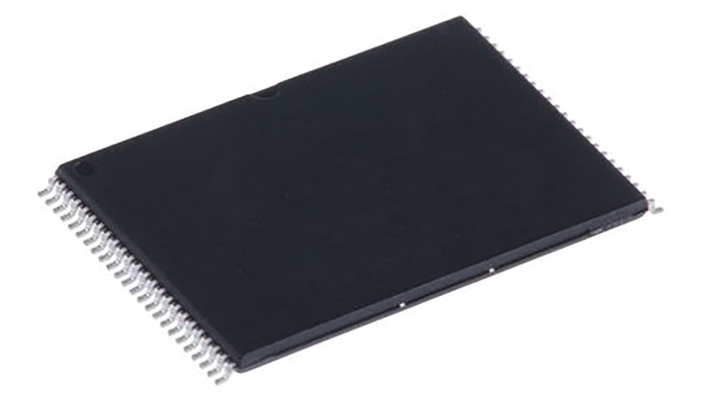
Cypress Semiconductor 32Mbit CFI Flash Memory 48-Pin TSOP, S29JL032J70TFI010
- RS Stock No.:
- 181-8288
- Mfr. Part No.:
- S29JL032J70TFI010
- Brand:
- Cypress Semiconductor

Stock information currently inaccessible
- RS Stock No.:
- 181-8288
- Mfr. Part No.:
- S29JL032J70TFI010
- Brand:
- Cypress Semiconductor
Specifications
Technical Reference
Legislation and Compliance
Product Details
Find similar products by selecting one or more attributes.
Select all | Attribute | Value |
|---|---|---|
| Brand | Cypress Semiconductor | |
| Memory Size | 32Mbit | |
| Interface Type | CFI | |
| Package Type | TSOP | |
| Pin Count | 48 | |
| Organisation | 4M x 8 bit | |
| Mounting Type | Surface Mount | |
| Minimum Operating Supply Voltage | 2.7 V | |
| Maximum Operating Supply Voltage | 3.6 V | |
| Dimensions | 18.4 x 12 x 1.05mm | |
| Number of Bits per Word | 8bit | |
| Minimum Operating Temperature | -40 °C | |
| Number of Words | 4M | |
| Maximum Operating Temperature | +85 °C | |
| Maximum Random Access Time | 70ns | |
| Number of Banks | 4 | |
| Select all | ||
|---|---|---|
Brand Cypress Semiconductor | ||
Memory Size 32Mbit | ||
Interface Type CFI | ||
Package Type TSOP | ||
Pin Count 48 | ||
Organisation 4M x 8 bit | ||
Mounting Type Surface Mount | ||
Minimum Operating Supply Voltage 2.7 V | ||
Maximum Operating Supply Voltage 3.6 V | ||
Dimensions 18.4 x 12 x 1.05mm | ||
Number of Bits per Word 8bit | ||
Minimum Operating Temperature -40 °C | ||
Number of Words 4M | ||
Maximum Operating Temperature +85 °C | ||
Maximum Random Access Time 70ns | ||
Number of Banks 4 | ||
Software Features
Supports Common Flash Memory Interface (CFI)
Erase suspend/Erase resume
Suspends erase operations to read data from, or program data to, a sector that is not being erased, then resumes the erase operation.
Data# polling and toggle bits
Provides a software method of detecting the status of pro-gram or erase operations
Unlock bypass program command Reduces overall programming time when issuing multiple program command sequences Hardware Features
Ready/Busy# output (RY/BY#)
Hardware method for detecting program or erase cycle completion
Hardware reset pin (RESET#)
Hardware method of resetting the internal state machine to the read mode
WP#/ACC input pin
Write protect (WP#) function protects the two outermost boot sectors regardless of sector protect status
Acceleration (ACC) function accelerates program timing
Sector protection
Hardware method to prevent any program or erase operation within a sector
Temporary Sector Unprotect allows changing data in protected sectors in-system