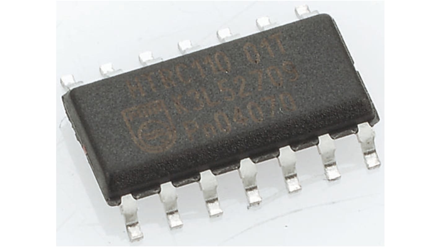
Nexperia HEF4094BT,652 8-stage Surface Mount Shift Register, 16-Pin SOIC
- RS Stock No.:
- 368-7874
- Mfr. Part No.:
- HEF4094BT,652
- Brand:
- Nexperia

Stock information currently inaccessible
- RS Stock No.:
- 368-7874
- Mfr. Part No.:
- HEF4094BT,652
- Brand:
- Nexperia
Specifications
Technical Reference
Legislation and Compliance
Product Details
Find similar products by selecting one or more attributes.
Select all | Attribute | Value |
|---|---|---|
| Brand | Nexperia | |
| Package Type | SOIC | |
| Logic Function | Shift Register | |
| Number of Stages | 8 | |
| Logic Family | 4000 | |
| Mounting Type | Surface Mount | |
| Operation Mode | Serial to Serial, Parallel | |
| Number of Elements | 1 | |
| Pin Count | 16 | |
| Minimum Operating Supply Voltage | 3 V | |
| Maximum Operating Supply Voltage | 15 V | |
| Dimensions | 10 x 4 x 1.45mm | |
| Triggering Type | Positive Edge | |
| Minimum Operating Temperature | -40 °C | |
| Maximum Operating Temperature | 125 °C | |
| Direction Type | Uni-Directional | |
| Select all | ||
|---|---|---|
Brand Nexperia | ||
Package Type SOIC | ||
Logic Function Shift Register | ||
Number of Stages 8 | ||
Logic Family 4000 | ||
Mounting Type Surface Mount | ||
Operation Mode Serial to Serial, Parallel | ||
Number of Elements 1 | ||
Pin Count 16 | ||
Minimum Operating Supply Voltage 3 V | ||
Maximum Operating Supply Voltage 15 V | ||
Dimensions 10 x 4 x 1.45mm | ||
Triggering Type Positive Edge | ||
Minimum Operating Temperature -40 °C | ||
Maximum Operating Temperature 125 °C | ||
Direction Type Uni-Directional | ||
The HEF4094B is an 8-stage serial shift register. It has a storage latch associated with each stage for strobing data from the serial input to parallel buffered 3‑state outputs QP0 to QP7. The parallel outputs may be connected directly to common bus lines. Data is shifted on positive‑going clock transitions. The data in each shift register stage is transferred to the storage register when the strobe (STR) input is HIGH. Data in the storage register appears at the outputs whenever the output enable (OE) signal is HIGH. Two serial outputs (QS1 and QS2) are available for cascading a number of HEF4094B devices. Serial data is available at QS1 on positive‑going clock edges to allow high‑speed operation in cascaded systems with a fast clock rise time.
Simple control interface
I/O expansion
Asynchronous and synchronous load options
High frequency
Cascadable
LED drivers
Key applications
Displays
Control units