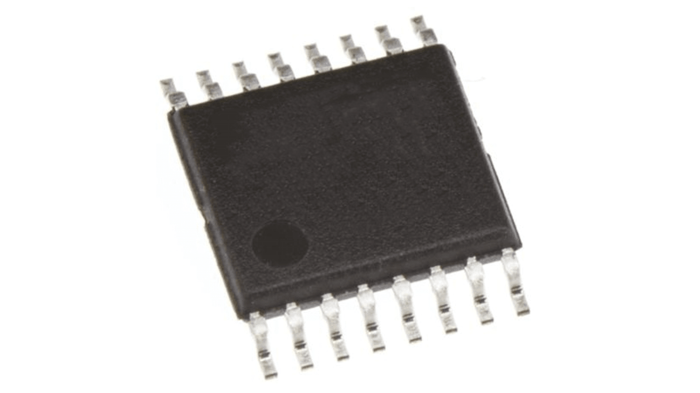
Renesas Electronics 5V2305PGGI Clock Buffer 16-Pin TSSOP, VFQFPN
- RS Stock No.:
- 254-4945P
- Mfr. Part No.:
- 5V2305PGGI
- Brand:
- Renesas Electronics

Bulk discount available
Subtotal 10 units (supplied in a tube)*
£26.40
(exc. VAT)
£31.70
(inc. VAT)
FREE delivery for orders over £50.00
In Stock
- 288 unit(s) ready to ship
Need more? Click ‘Check delivery dates’ to find extra stock and lead times.
Units | Per unit |
|---|---|
| 10 - 18 | £2.64 |
| 20 - 48 | £2.59 |
| 50 - 94 | £2.50 |
| 96 + | £2.16 |
*price indicative
- RS Stock No.:
- 254-4945P
- Mfr. Part No.:
- 5V2305PGGI
- Brand:
- Renesas Electronics
Specifications
Technical Reference
Legislation and Compliance
Product Details
Find similar products by selecting one or more attributes.
Select all | Attribute | Value |
|---|---|---|
| Brand | Renesas Electronics | |
| Number of Elements per Chip | 5 | |
| Maximum Supply Current | 50 mA | |
| Maximum Input Frequency | 200MHz | |
| Mounting Type | Surface Mount | |
| Package Type | TSSOP, VFQFPN | |
| Pin Count | 16 | |
| Select all | ||
|---|---|---|
Brand Renesas Electronics | ||
Number of Elements per Chip 5 | ||
Maximum Supply Current 50 mA | ||
Maximum Input Frequency 200MHz | ||
Mounting Type Surface Mount | ||
Package Type TSSOP, VFQFPN | ||
Pin Count 16 | ||
The Renesas Electronics high performance, low skew clock buffer that operates up to 200 MHz. One bank of five outputs provides low skew copies of CLK. Through the use of control pin G, the outputs of bank Y(0:4) can be placed in a low state regardless of CLK input. The device operates in 2.5 V and 3.3 V environments. The built-in output enable glitch suppression ensures a synchronized output enable sequence to distribute full period clock signals. It is is characterized for operation from -40°C to +85°C.
High performance 1:5 clock driver for general purpose applications
Operates up to 170 MHz at VDD is 2.5 V
Operates up to 200 MHz at VDD is 3.3 V
Pin-to-pin skew < 75 ps at 3.3 V operation
VDD range is 2.3 V to 3.6 V
Output enable glitch suppression
Available in TSSOP and VFQFPN packages
Operates up to 170 MHz at VDD is 2.5 V
Operates up to 200 MHz at VDD is 3.3 V
Pin-to-pin skew < 75 ps at 3.3 V operation
VDD range is 2.3 V to 3.6 V
Output enable glitch suppression
Available in TSSOP and VFQFPN packages