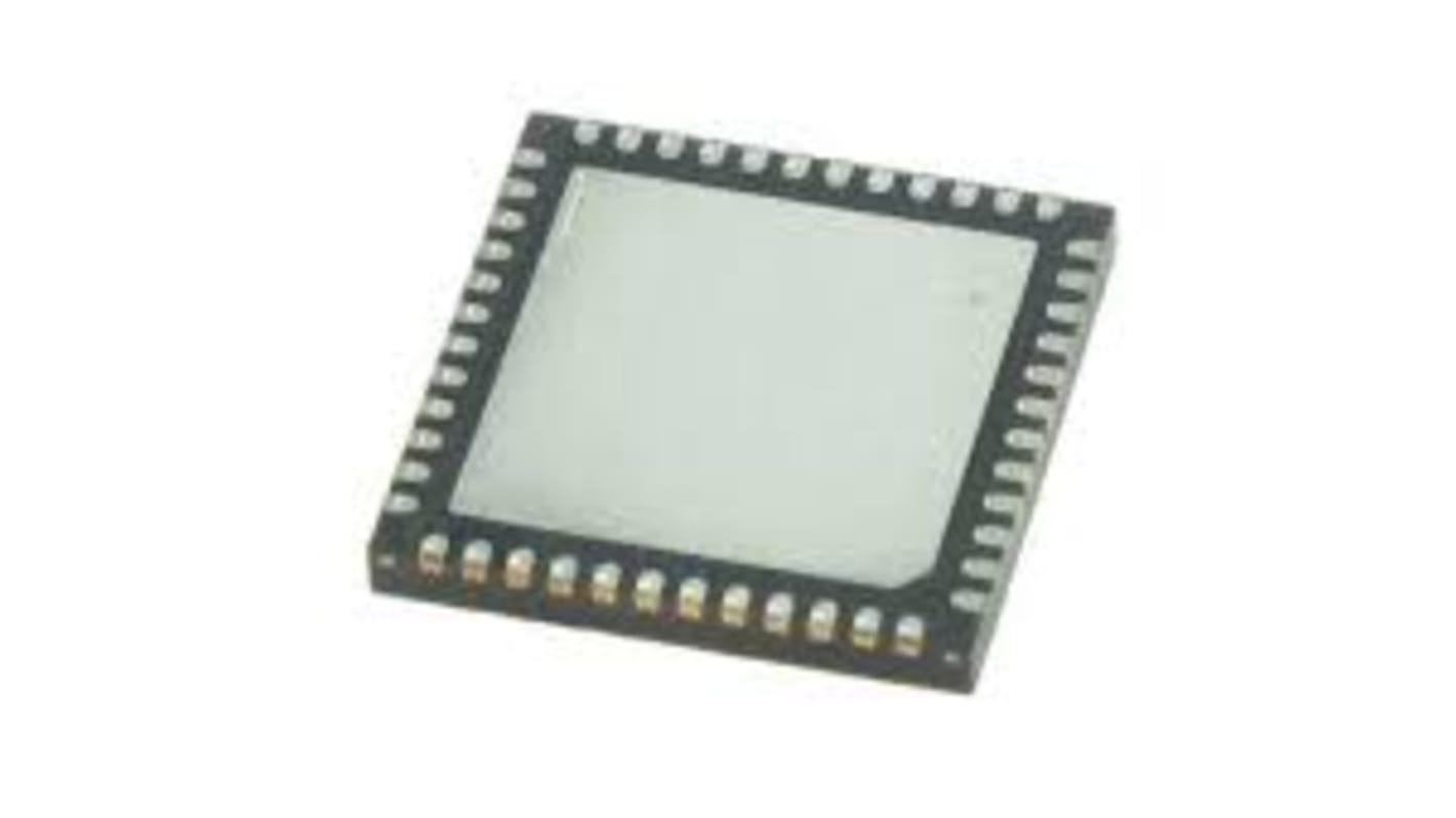
Renesas Electronics 9DBL0951BKILF Clock Buffer 48-Pin VFQFPN
- RS Stock No.:
- 250-3487P
- Mfr. Part No.:
- 9DBL0951BKILF
- Brand:
- Renesas Electronics

Bulk discount available
Subtotal 10 units (supplied in a tray)*
£21.45
(exc. VAT)
£25.74
(inc. VAT)
FREE delivery for orders over £50.00
In Stock
- 356 unit(s) ready to ship
Need more? Click ‘Check delivery dates’ to find extra stock and lead times.
Units | Per unit |
|---|---|
| 10 - 18 | £2.145 |
| 20 - 98 | £2.10 |
| 100 - 198 | £1.745 |
| 200 + | £1.715 |
*price indicative
- RS Stock No.:
- 250-3487P
- Mfr. Part No.:
- 9DBL0951BKILF
- Brand:
- Renesas Electronics
Specifications
Technical Reference
Legislation and Compliance
Product Details
Find similar products by selecting one or more attributes.
Select all | Attribute | Value |
|---|---|---|
| Brand | Renesas Electronics | |
| Maximum Supply Current | 40 mA | |
| Maximum Input Frequency | 200MHz | |
| Mounting Type | Surface Mount | |
| Package Type | VFQFPN | |
| Pin Count | 48 | |
| Select all | ||
|---|---|---|
Brand Renesas Electronics | ||
Maximum Supply Current 40 mA | ||
Maximum Input Frequency 200MHz | ||
Mounting Type Surface Mount | ||
Package Type VFQFPN | ||
Pin Count 48 | ||
The Renesas Electronics fan-out buffers are 3.3V members of IDT's full featured PCIe clock family. This devices support PCIe Gen1–4 Common Clocked (CC) and PCIe
Separate Reference Independent Spread (SRIS) systems. They offer a choice of integrated output terminations providing direct connection to 85Ω or 100Ω transmission lines. It can be factory programmed with a user-defined power up default SMBus configuration. Various applications where this device is used are PCIe Gen1–4 clock distribution for Riser Cards, Storage, Networking, JBOD, Communications and Access Points.
Separate Reference Independent Spread (SRIS) systems. They offer a choice of integrated output terminations providing direct connection to 85Ω or 100Ω transmission lines. It can be factory programmed with a user-defined power up default SMBus configuration. Various applications where this device is used are PCIe Gen1–4 clock distribution for Riser Cards, Storage, Networking, JBOD, Communications and Access Points.
Direct connection to 100ohm or 85ohm transmission lines saves 36 resistors compared to standard PCIe devices
165mW of typical power consumption at 3.3V eliminates thermal concerns
VDDIO allows 50% power savings at optional 1.05V
Customer defined SMBus power up default can be programmed into P1 device
HCSL differential input can be driven by common clock sources
Spread spectrum tolerant allows reduction of EMI
Device contains default configuration
Three selectable SMBus addresses so multiple devices can easily share an SMBus segment
Space saving 48-pin 6 x 6mm VFQFPN