Nexperia 74LVC1G17GW-Q100,1 Schmitt Trigger CMOS Schmitt Buffer, 5-Pin TSSOP
- RS Stock No.:
- 152-6475
- Mfr. Part No.:
- 74LVC1G17GW-Q100,1
- Brand:
- Nexperia

Stock information currently inaccessible
- RS Stock No.:
- 152-6475
- Mfr. Part No.:
- 74LVC1G17GW-Q100,1
- Brand:
- Nexperia
Specifications
Technical Reference
Legislation and Compliance
Product Details
Find similar products by selecting one or more attributes.
Select all | Attribute | Value |
|---|---|---|
| Brand | Nexperia | |
| Logic Family | 74LVC | |
| Logic Function | Schmitt Trigger Buffer | |
| Number of Channels | 1 | |
| Schmitt Trigger Input | Yes | |
| Input Type | Schmitt Trigger | |
| Output Type | CMOS | |
| Mounting Type | Surface Mount | |
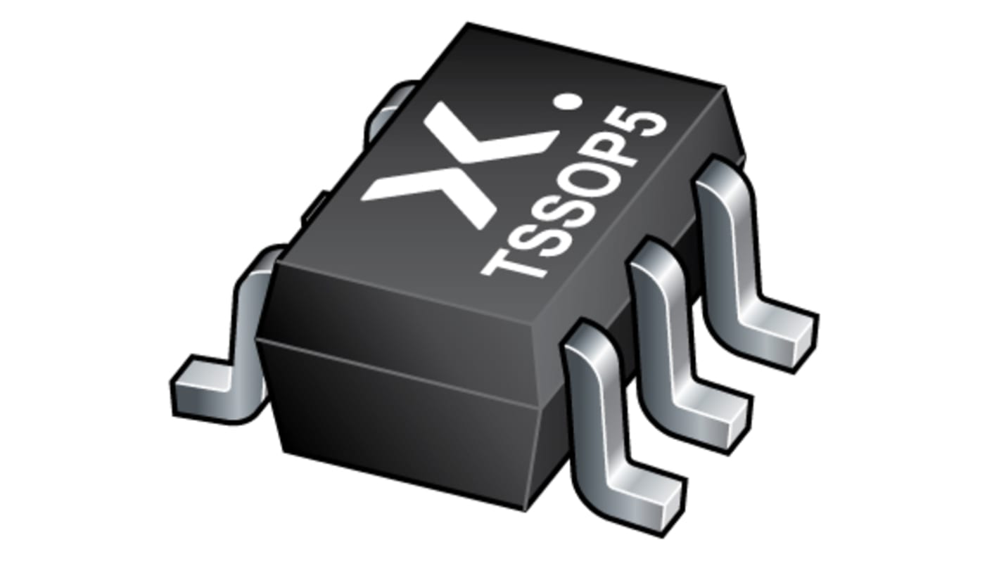
| Package Type | TSSOP | |
| Pin Count | 5 | |
| Maximum High Level Output Current | -32mA | |
| Maximum Low Level Output Current | -32mA | |
| Dimensions | 2.25 x 1.35 x 1mm | |
| Maximum Operating Supply Voltage | 5.5 V | |
| Minimum Operating Supply Voltage | 1.65 V | |
| Length | 2.25mm | |
| Automotive Standard | AEC-Q100 | |
| Maximum Operating Temperature | +125 °C | |
| Width | 1.35mm | |
| Height | 1mm | |
| Minimum Operating Temperature | -40 °C | |
| Select all | ||
|---|---|---|
Brand Nexperia | ||
Logic Family 74LVC | ||
Logic Function Schmitt Trigger Buffer | ||
Number of Channels 1 | ||
Schmitt Trigger Input Yes | ||
Input Type Schmitt Trigger | ||
Output Type CMOS | ||
Mounting Type Surface Mount | ||
Package Type TSSOP | ||
Pin Count 5 | ||
Maximum High Level Output Current -32mA | ||
Maximum Low Level Output Current -32mA | ||
Dimensions 2.25 x 1.35 x 1mm | ||
Maximum Operating Supply Voltage 5.5 V | ||
Minimum Operating Supply Voltage 1.65 V | ||
Length 2.25mm | ||
Automotive Standard AEC-Q100 | ||
Maximum Operating Temperature +125 °C | ||
Width 1.35mm | ||
Height 1mm | ||
Minimum Operating Temperature -40 °C | ||
Single Schmitt trigger buffer, The 74LVC1G17-Q100 provides a buffer function with Schmitt trigger input. It is capable of transforming slowly changing input signals into sharply defined outputs. The input can be driven from either 3.3 V or 5 V devices. This feature allows the use of this device in a mixed 3.3 V and 5 V environment. This device is fully specified for partial power-down applications using IOFF. The IOFF circuitry disables the output, preventing the damaging backflow current through the device when it is powered down.
Automotive product qualification in accordance with AEC-Q100 (Grade 1)
Specified from -40 °C to +85 °C and from -40 °C to +125 °C
Wide supply voltage range from 1.65 V to 5.5 V
High noise immunity
Specified from -40 °C to +85 °C and from -40 °C to +125 °C
Wide supply voltage range from 1.65 V to 5.5 V
High noise immunity