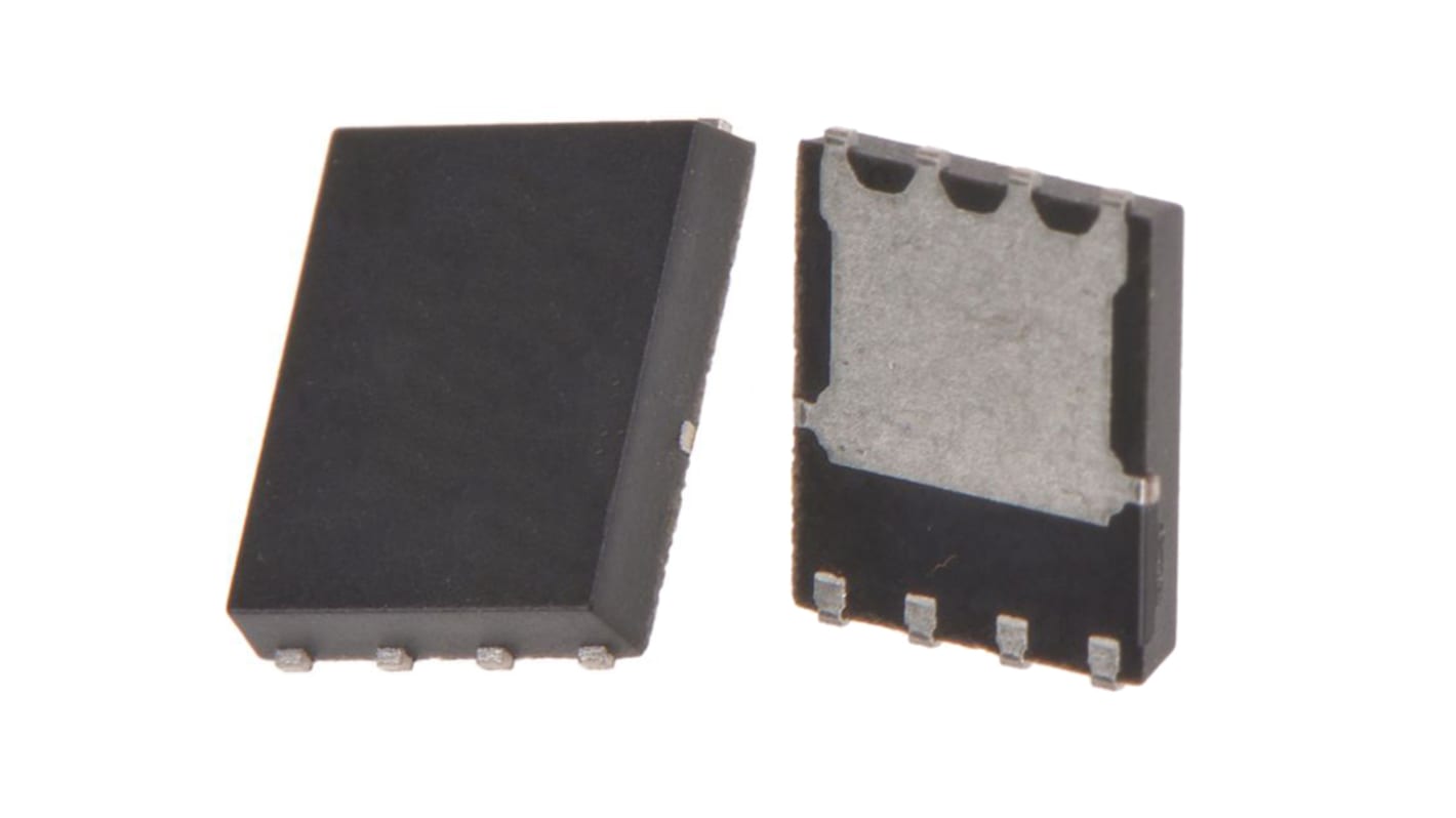
ON Semi FDMS3624S Dual Digital Transistor, 8-Pin PQFN
- RS Stock No.:
- 186-7156
- Mfr. Part No.:
- FDMS3624S
- Brand:
- ON Semiconductor

Unavailable
RS will no longer stock this product.
- RS Stock No.:
- 186-7156
- Mfr. Part No.:
- FDMS3624S
- Brand:
- ON Semiconductor
Specifications
Technical Reference
Legislation and Compliance
Product Details
Find similar products by selecting one or more attributes.
Select all | Attribute | Value |
|---|---|---|
| Brand | ON Semiconductor | |
| Package Type | PQFN | |
| Mounting Type | Surface Mount | |
| Maximum Power Dissipation | 2.5 W | |
| Pin Count | 8 | |
| Number of Elements per Chip | 2 | |
| Maximum Operating Temperature | +150 °C | |
| Dimensions | 6.25 x 5.1 x 1.05mm | |
| Select all | ||
|---|---|---|
Brand ON Semiconductor | ||
Package Type PQFN | ||
Mounting Type Surface Mount | ||
Maximum Power Dissipation 2.5 W | ||
Pin Count 8 | ||
Number of Elements per Chip 2 | ||
Maximum Operating Temperature +150 °C | ||
Dimensions 6.25 x 5.1 x 1.05mm | ||
This device includes two specialized N-Channel MOSFETs in a dual PQFN package. The switch node has been internally connected to enable easy placement and routing of synchronous buck converters. The control MOSFET (Q1) and synchronousSyncFET (Q2) have been designed to provide optimal power efficiency.
Q1: N-Channel
Max rDS(on) = 5.0 mΩ at VGS = 10 V, ID = 17.5 A
Max rDS(on) = 5.7 mΩ at VGS = 4.5 V, ID = 16 A
Q2: N-Channel
Max rDS(on) = 1.8 mΩ at VGS = 10 V, ID = 30 A
Max rDS(on) = 2.2 mΩ at VGS = 4.5 V, ID = 27 A
Low inductance packaging shortens rise/fall times, resulting in lower switching losses
MOSFET integration enables optimum layout for lower circuit inductance and reduced switch node ringing
Applications
Distribution
Notebook PC