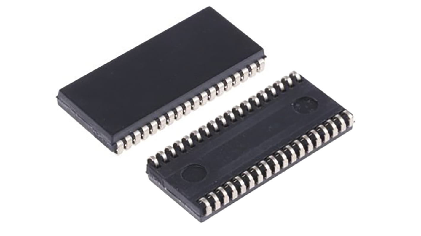
Infineon SRAM Memory Chip, CY7C1049GN-10VXI- 4Mbit
- RS Stock No.:
- 182-3295
- Mfr. Part No.:
- CY7C1049GN-10VXI
- Brand:
- Infineon

Subtotal (1 tube of 19 units)*
£100.51
(exc. VAT)
£120.65
(inc. VAT)
FREE delivery for orders over £50.00
Temporarily out of stock
- Shipping from 26 January 2026
Need more? Click ‘Check delivery dates’ to find extra stock and lead times.
Units | Per unit | Per Tube* |
|---|---|---|
| 19 + | £5.29 | £100.51 |
*price indicative
- RS Stock No.:
- 182-3295
- Mfr. Part No.:
- CY7C1049GN-10VXI
- Brand:
- Infineon
Specifications
Technical Reference
Legislation and Compliance
Product Details
Find similar products by selecting one or more attributes.
Select all | Attribute | Value |
|---|---|---|
| Brand | Infineon | |
| Memory Size | 4Mbit | |
| Organisation | 512k x 16 bit | |
| Number of Words | 512k | |
| Number of Bits per Word | 8bit | |
| Maximum Random Access Time | 10ns | |
| Clock Frequency | 100MHz | |
| Timing Type | Asynchronous | |
| Mounting Type | Surface Mount | |
| Package Type | SOJ | |
| Pin Count | 36 | |
| Dimensions | 0.93 x 0.4 x 0.12mm | |
| Height | 0.12mm | |
| Maximum Operating Supply Voltage | 5.5 V | |
| Length | 0.93mm | |
| Maximum Operating Temperature | +85 °C | |
| Minimum Operating Supply Voltage | 4.5 V | |
| Minimum Operating Temperature | -40 °C | |
| Width | 0.4mm | |
Select all | ||
|---|---|---|
Brand Infineon | ||
Memory Size 4Mbit | ||
Organisation 512k x 16 bit | ||
Number of Words 512k | ||
Number of Bits per Word 8bit | ||
Maximum Random Access Time 10ns | ||
Clock Frequency 100MHz | ||
Timing Type Asynchronous | ||
Mounting Type Surface Mount | ||
Package Type SOJ | ||
Pin Count 36 | ||
Dimensions 0.93 x 0.4 x 0.12mm | ||
Height 0.12mm | ||
Maximum Operating Supply Voltage 5.5 V | ||
Length 0.93mm | ||
Maximum Operating Temperature +85 °C | ||
Minimum Operating Supply Voltage 4.5 V | ||
Minimum Operating Temperature -40 °C | ||
Width 0.4mm | ||
- COO (Country of Origin):
- US
CY7C1049GN is a high-performance CMOS fast static RAM device organized as 512K words by 8-bits. Data writes are performed by asserting the Chip Enable (CE) and Write Enable (WE) inputs LOW, while providing the data on I/O0 through I/O7 and address on A0 through A18 pins. Data reads are performed by asserting the Chip Enable (CE) and Output Enable (OE) inputs LOW and providing the required address on the address lines. Read data is accessible on the I/O lines (I/O0 through I/O7). All I/Os (I/O0 through I/O7) are placed in a high-impedance state during the following events: The device is deselected (CE HIGH) The control signal OE is de-asserted.
High speed
tAA = 10 ns
Low active and standby currents
Active current: ICC = 38 mA typical
Standby current: ISB2 = 6 mA typical
Operating voltage range: 1.65 V to 2.2 V, 2.2 V to 3.6 V, and
4.5 V to 5.5 V
1.0 V data retention
TTL-compatible inputs and outputs
Pb-free 36-pin SOJ and 44-pin TSOP II packages
tAA = 10 ns
Low active and standby currents
Active current: ICC = 38 mA typical
Standby current: ISB2 = 6 mA typical
Operating voltage range: 1.65 V to 2.2 V, 2.2 V to 3.6 V, and
4.5 V to 5.5 V
1.0 V data retention
TTL-compatible inputs and outputs
Pb-free 36-pin SOJ and 44-pin TSOP II packages