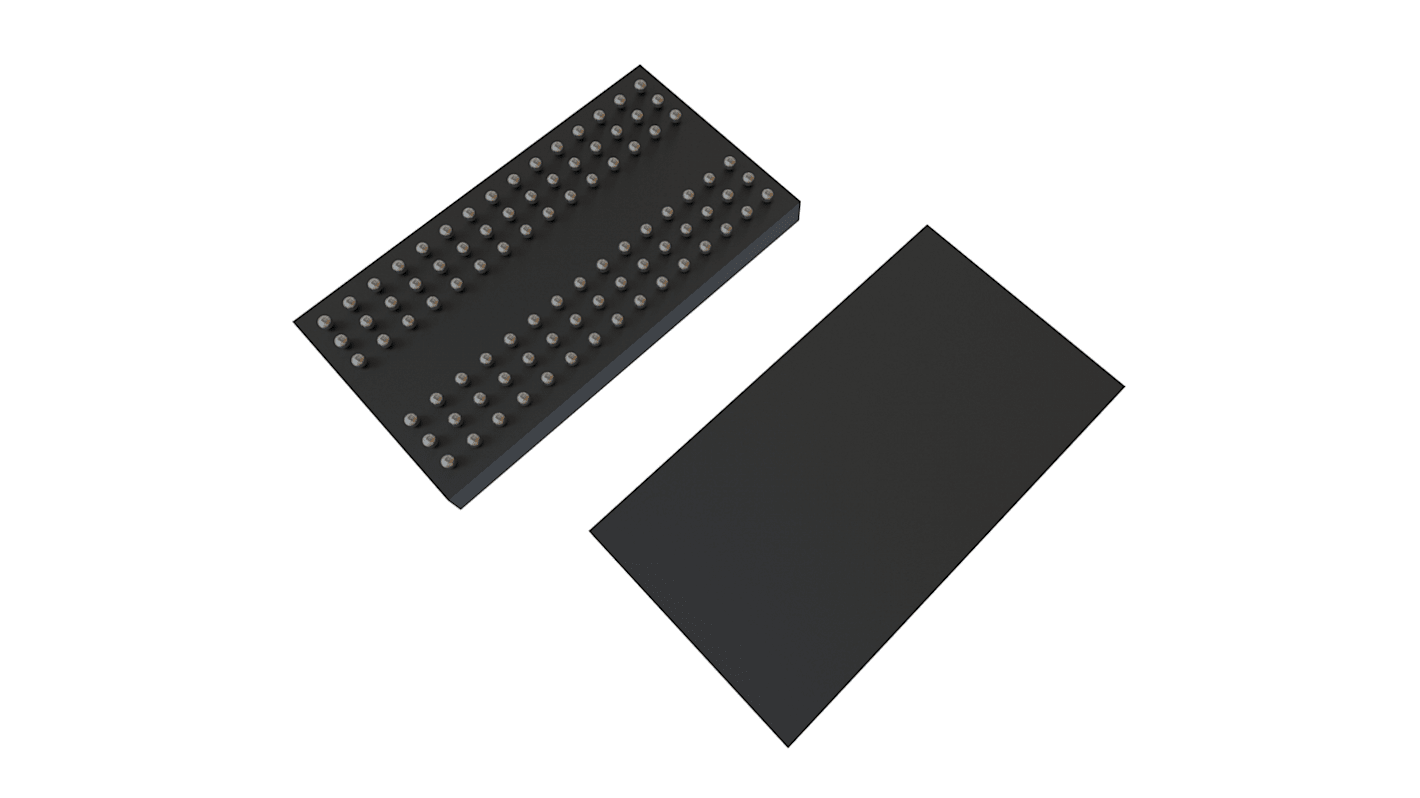
Winbond W9751G8KB25I, SDRAM 512Mbit Surface Mount, 60-Pin WBGA
- RS Stock No.:
- 188-2642
- Mfr. Part No.:
- W9751G8KB25I
- Brand:
- Winbond

Bulk discount available
Subtotal (1 pack of 5 units)*
£11.98
(exc. VAT)
£14.375
(inc. VAT)
Stock information currently inaccessible - Please check back later
Units | Per unit | Per Pack* |
|---|---|---|
| 5 - 5 | £2.396 | £11.98 |
| 10 - 15 | £2.166 | £10.83 |
| 20 - 45 | £2.122 | £10.61 |
| 50 - 95 | £2.116 | £10.58 |
| 100 + | £1.892 | £9.46 |
*price indicative
- RS Stock No.:
- 188-2642
- Mfr. Part No.:
- W9751G8KB25I
- Brand:
- Winbond
Specifications
Technical Reference
Legislation and Compliance
Product Details
Find similar products by selecting one or more attributes.
Select all | Attribute | Value |
|---|---|---|
| Brand | Winbond | |
| Memory Size | 512Mbit | |
| Organisation | 64M x 8 bit | |
| Number of Bits per Word | 8bit | |
| Number of Words | 64M | |
| Mounting Type | Surface Mount | |
| Package Type | WBGA | |
| Pin Count | 60 | |
| Dimensions | 12.6 x 8.1 x 0.6mm | |
| Height | 0.6mm | |
| Length | 12.6mm | |
| Width | 8.1mm | |
| Minimum Operating Supply Voltage | 1.7 V | |
| Maximum Operating Supply Voltage | 1.9 V | |
| Maximum Operating Temperature | +95 °C | |
| Minimum Operating Temperature | -40 °C | |
| Select all | ||
|---|---|---|
Brand Winbond | ||
Memory Size 512Mbit | ||
Organisation 64M x 8 bit | ||
Number of Bits per Word 8bit | ||
Number of Words 64M | ||
Mounting Type Surface Mount | ||
Package Type WBGA | ||
Pin Count 60 | ||
Dimensions 12.6 x 8.1 x 0.6mm | ||
Height 0.6mm | ||
Length 12.6mm | ||
Width 8.1mm | ||
Minimum Operating Supply Voltage 1.7 V | ||
Maximum Operating Supply Voltage 1.9 V | ||
Maximum Operating Temperature +95 °C | ||
Minimum Operating Temperature -40 °C | ||
The W9751G8KB is a 512M bits DDR2 SDRAM, and speed involving -18/-25/25I and -3.
Double Data Rate architecture: two data transfers per clock cycle
CAS Latency: 3, 4, 5, 6 and 7
Burst Length: 4 and 8
Bi-directional, differential data strobes (DQS and /DQS ) are transmitted / received with data
Edge-aligned with Read data and center-aligned with Write data
DLL aligns DQ and DQS transitions with clock
Differential clock inputs (CLK and /CLK)
Data masks (DM) for write data
Commands entered on each positive CLK edge, data and data mask are referenced to both edges of /DQS
Posted /CAS programmable additive latency supported to make command and data bus efficiency
Read Latency = Additive Latency plus CAS Latency (RL = AL + CL)
Off-Chip-Driver impedance adjustment (OCD) and On-Die-Termination (ODT) for better signal quality
Auto-precharge operation for read and write bursts
Auto Refresh and Self Refresh modes
Precharged Power Down and Active Power Down
Write Data Mask
Write Latency = Read Latency - 1 (WL = RL - 1)
Interface: SSTL_18