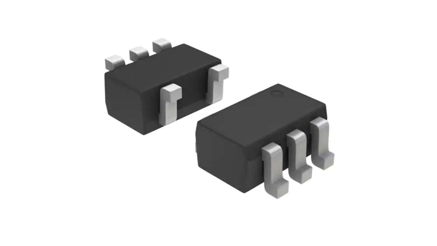
onsemi, 1 1-Input AND Logic Gate, 5-Pin SOT-353
- RS Stock No.:
- 184-4783P
- Mfr. Part No.:
- M74VHC1GT08DFT2G
- Brand:
- onsemi

Bulk discount available
Subtotal 500 units (supplied on a reel)*
£42.50
(exc. VAT)
£51.00
(inc. VAT)
FREE delivery for orders over £60.00
Last RS stock
- Final 2,400 unit(s), ready to ship
Units | Per unit |
|---|---|
| 500 - 900 | £0.085 |
| 1000 + | £0.074 |
*price indicative
- RS Stock No.:
- 184-4783P
- Mfr. Part No.:
- M74VHC1GT08DFT2G
- Brand:
- onsemi
Specifications
Technical Reference
Legislation and Compliance
Product Details
Find similar products by selecting one or more attributes.
Select all | Attribute | Value |
|---|---|---|
| Brand | onsemi | |
| Product Type | Logic Gate | |
| Logic Function | AND | |
| Mount Type | Surface | |
| Number of Elements | 1 | |
| Number of Inputs per Gate | 1 | |
| Package Type | SOT-353 | |
| Pin Count | 5 | |
| Logic Family | 74VHC | |
| Input Type | TTL, CMOS | |
| Maximum High Level Output Current | -8mA | |
| Maximum Propagation Delay Time @ CL | 11ns | |
| Minimum Operating Temperature | -55°C | |
| Maximum Operating Temperature | 125°C | |
| Length | 2.2mm | |
| Height | 1mm | |
| Minimum Supply Voltage | 2V | |
| Maximum Supply Voltage | 5.5V | |
| Standards/Approvals | No | |
| Maximum Low Level Output Current | 8mA | |
| Automotive Standard | AEC-Q100 | |
| Select all | ||
|---|---|---|
Brand onsemi | ||
Product Type Logic Gate | ||
Logic Function AND | ||
Mount Type Surface | ||
Number of Elements 1 | ||
Number of Inputs per Gate 1 | ||
Package Type SOT-353 | ||
Pin Count 5 | ||
Logic Family 74VHC | ||
Input Type TTL, CMOS | ||
Maximum High Level Output Current -8mA | ||
Maximum Propagation Delay Time @ CL 11ns | ||
Minimum Operating Temperature -55°C | ||
Maximum Operating Temperature 125°C | ||
Length 2.2mm | ||
Height 1mm | ||
Minimum Supply Voltage 2V | ||
Maximum Supply Voltage 5.5V | ||
Standards/Approvals No | ||
Maximum Low Level Output Current 8mA | ||
Automotive Standard AEC-Q100 | ||
- COO (Country of Origin):
- CN
The MC74VHC1GT08 is an advanced high speed CMOS 2-input AND gate fabricated with silicon gate CMOS technology. It achieves high speed operation similar to equivalent Bipolar Schottky TTL while maintaining CMOS low power dissipation. The internal circuit is composed of three stages, including a buffer output which provides high noise immunity and stable output. The device input is compatible with TTL-type input thresholds and the output has a full 5 V CMOS level output swing. The input protection circuitry on this device allows overvoltage tolerance on the input, allowing the device to be used as a logic-level translator from 3.0 V CMOS logic to 5.0 V CMOS Logic or from 1.8 V CMOS logic to 3.0 V CMOS Logic while operating at the high-voltage power supply. The MC74VHC1GT08 input structure provides protection when voltages up to 7 V are applied, regardless of the supply voltage. This allows the MC74VHC1GT08 to be used to interface 5 V circuits to 3 V circuits. The output structures also provide protection when VCC = 0 V. These input and output structures help prevent device destruction caused by supply voltage - input/output voltage mismatch, battery backup, hot insertion, etc.