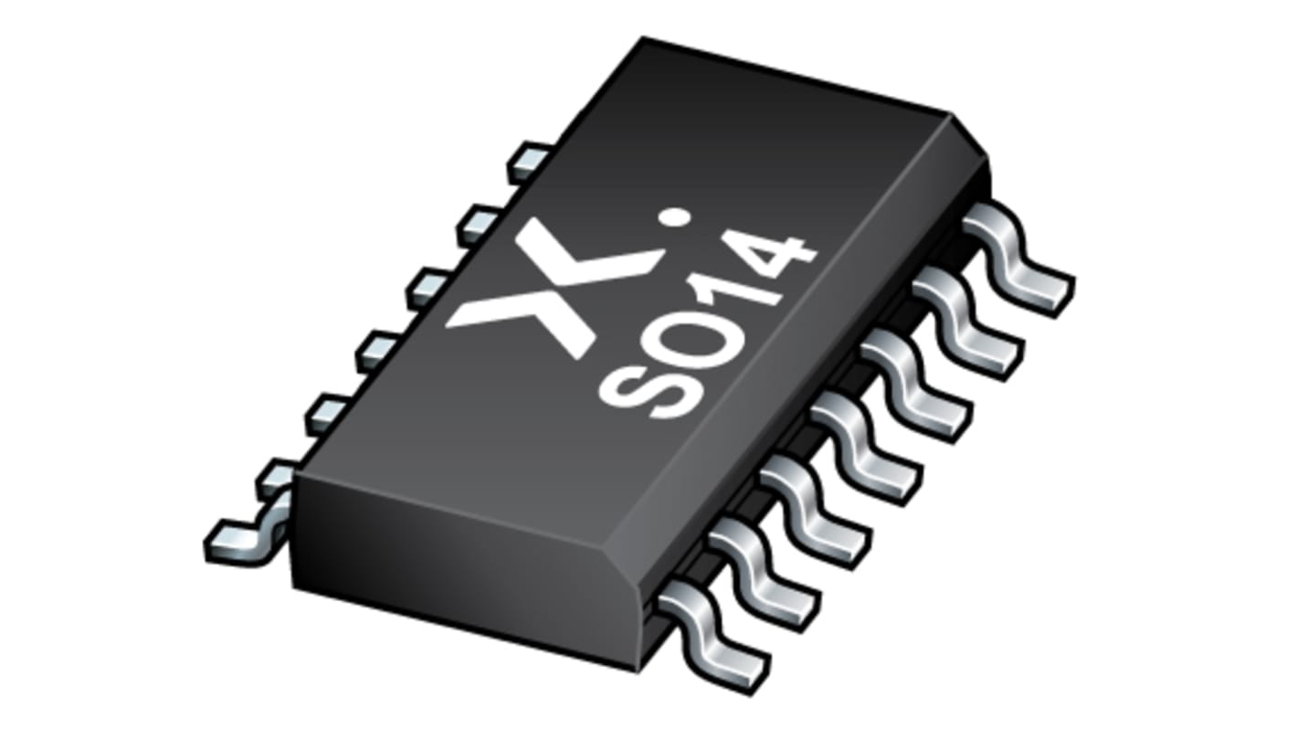
Nexperia HEF4073BT,653, Triple 3-Input AND Logic Gate, 14-PinSOIC
- RS Stock No.:
- 170-4883
- Mfr. Part No.:
- HEF4073BT,653
- Brand:
- Nexperia

Stock information currently inaccessible
- RS Stock No.:
- 170-4883
- Mfr. Part No.:
- HEF4073BT,653
- Brand:
- Nexperia
Specifications
Technical Reference
Legislation and Compliance
Product Details
Find similar products by selecting one or more attributes.
Select all | Attribute | Value |
|---|---|---|
| Brand | Nexperia | |
| Logic Function | AND | |
| Mounting Type | Surface Mount | |
| Number of Elements | 3 | |
| Number of Inputs per Gate | 3 | |
| Package Type | SO | |
| Pin Count | 14 | |
| Logic Family | HEF | |
| Input Type | CMOS | |
| Maximum Operating Supply Voltage | 15 V | |
| Maximum High Level Output Current | -2.4mA | |
| Maximum Propagation Delay Time @ Maximum CL | 110 ns @ 50 pF | |
| Minimum Operating Supply Voltage | 3 V | |
| Maximum Low Level Output Current | 2.4mA | |
| Output Type | Buffer | |
| Minimum Operating Temperature | -40 °C | |
| Propagation Delay Test Condition | 50pF | |
| Length | 8.75mm | |
| Dimensions | 8.75 x 4 x 1.45mm | |
| Maximum Operating Temperature | +85 °C | |
| Height | 1.45mm | |
| Width | 4mm | |
| Select all | ||
|---|---|---|
Brand Nexperia | ||
Logic Function AND | ||
Mounting Type Surface Mount | ||
Number of Elements 3 | ||
Number of Inputs per Gate 3 | ||
Package Type SO | ||
Pin Count 14 | ||
Logic Family HEF | ||
Input Type CMOS | ||
Maximum Operating Supply Voltage 15 V | ||
Maximum High Level Output Current -2.4mA | ||
Maximum Propagation Delay Time @ Maximum CL 110 ns @ 50 pF | ||
Minimum Operating Supply Voltage 3 V | ||
Maximum Low Level Output Current 2.4mA | ||
Output Type Buffer | ||
Minimum Operating Temperature -40 °C | ||
Propagation Delay Test Condition 50pF | ||
Length 8.75mm | ||
Dimensions 8.75 x 4 x 1.45mm | ||
Maximum Operating Temperature +85 °C | ||
Height 1.45mm | ||
Width 4mm | ||
- COO (Country of Origin):
- TH
The HEF4073B is a triple 3-input AND gate. The outputs are fully buffered for highest noise immunity and pattern insensitivity to output impedance variations. It operates over a recommended VDD power supply range of 3 V to 15 V referenced to VSS (usually ground). Unused inputs must be connected to VDD, VSS, or another input.
Mixed 5 V and 3.3 V applications
Reduce time to market for complex designs
Save board space
Open-drain output options
Improved signal integrity for complex layouts
Wide supply voltage range
Low propagation delay
Overvoltage tolerant options
Low input threshold options
CMOS low power
Key applications
Cell phone
Computing
STB
LCD TV
Industrial controllers