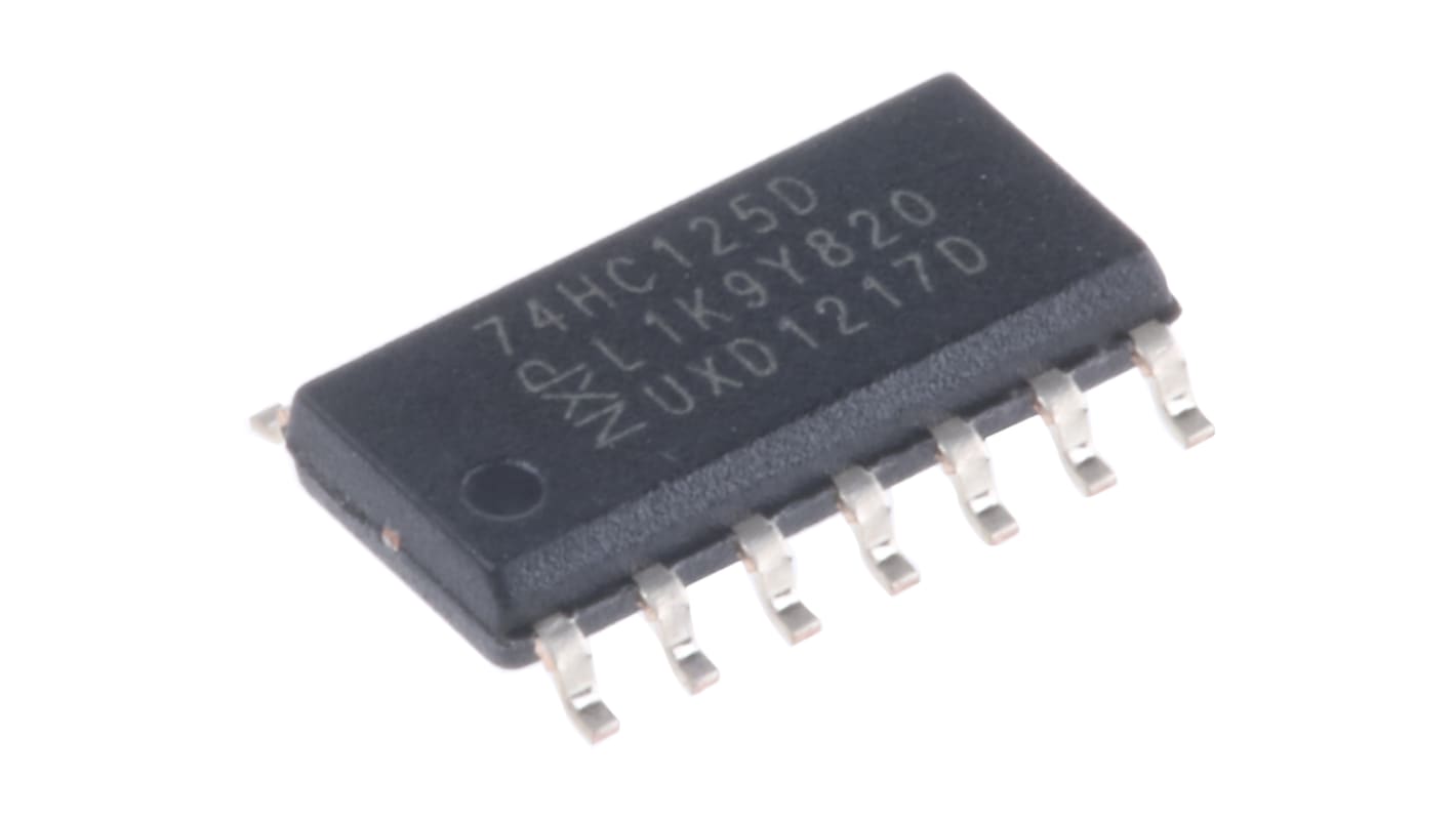
Nexperia 74HC125D,652 Buffer, Line Driver Logic Gate, 14-Pin SOIC
- RS Stock No.:
- 113-0528
- Mfr. Part No.:
- 74HC125D,652
- Brand:
- Nexperia
Currently unavailable
We don't know if this item will be back in stock, RS intend to remove it from our range soon.
- RS Stock No.:
- 113-0528
- Mfr. Part No.:
- 74HC125D,652
- Brand:
- Nexperia
Specifications
Technical Reference
Legislation and Compliance
Product Details
Find similar products by selecting one or more attributes.
Select all | Attribute | Value |
|---|---|---|
| Brand | Nexperia | |
| Logic Function | Buffer, Line Driver | |
| Mounting Type | Surface Mount | |
| Schmitt Trigger Input | No | |
| Package Type | SOIC | |
| Pin Count | 14 | |
| Logic Family | HC | |
| Input Type | Single Ended | |
| Maximum Operating Supply Voltage | 6 V | |
| Maximum High Level Output Current | -7.8mA | |
| Maximum Propagation Delay Time @ Maximum CL | 100 ns @ 2 V | |
| Minimum Operating Supply Voltage | 2 V | |
| Maximum Low Level Output Current | 7.8mA | |
| Length | 8.75mm | |
| Minimum Operating Temperature | -40 °C | |
| Width | 4mm | |
| Output Type | 3 State | |
| Dimensions | 8.75 x 4 x 1.45mm | |
| Maximum Operating Temperature | +125 °C | |
| Height | 1.45mm | |
| Propagation Delay Test Condition | 50pF | |
| Select all | ||
|---|---|---|
Brand Nexperia | ||
Logic Function Buffer, Line Driver | ||
Mounting Type Surface Mount | ||
Schmitt Trigger Input No | ||
Package Type SOIC | ||
Pin Count 14 | ||
Logic Family HC | ||
Input Type Single Ended | ||
Maximum Operating Supply Voltage 6 V | ||
Maximum High Level Output Current -7.8mA | ||
Maximum Propagation Delay Time @ Maximum CL 100 ns @ 2 V | ||
Minimum Operating Supply Voltage 2 V | ||
Maximum Low Level Output Current 7.8mA | ||
Length 8.75mm | ||
Minimum Operating Temperature -40 °C | ||
Width 4mm | ||
Output Type 3 State | ||
Dimensions 8.75 x 4 x 1.45mm | ||
Maximum Operating Temperature +125 °C | ||
Height 1.45mm | ||
Propagation Delay Test Condition 50pF | ||
The 74HC125, 74HCT125 is a quad buffer/line driver with 3-state outputs controlled by the output enable inputs (nOE). A HIGH on nOE causes the outputs to assume a high impedance OFF-state. Inputs include clamp diodes. This enables the use of current limiting resistors to interface inputs to voltages in excess of VCC.
Mixed 5 V and 3.3 V applications
Improved current drive and voltage level of signals
Improved signal integrity for complex layouts
Wide supply voltage range
Low propagation delay
TTL input options
3-state output options
Overvoltage tolerant options
Registered options
Key applications
LCD TV
Cell phones
Industrial monitoring
STB
