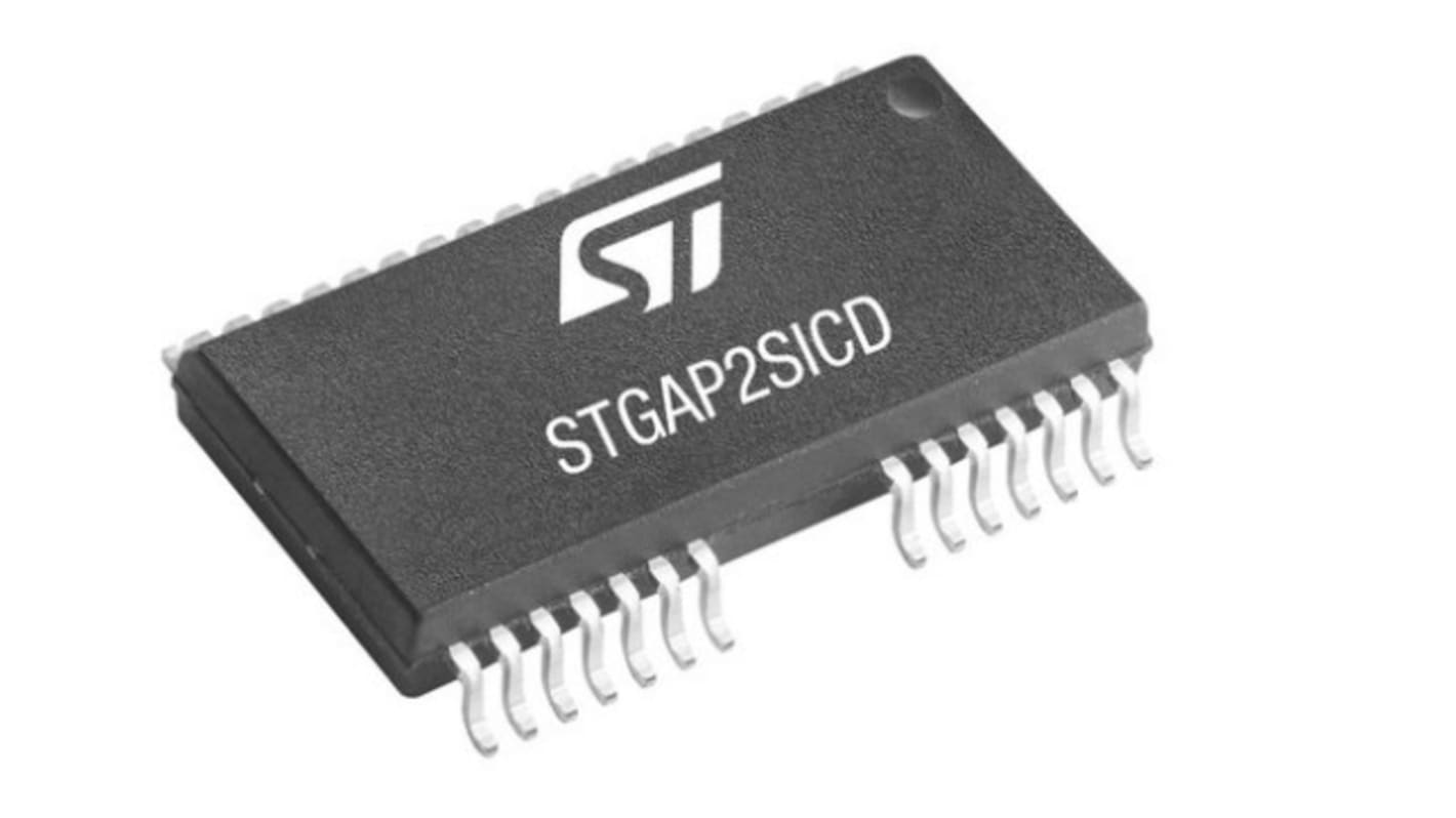
STMicroelectronics STGAP2SICDTR MOSFET Gate Driver, 4 A, 3.1 V, 5.5 V 36-Pin, SO-36W
- RS Stock No.:
- 239-5534
- Mfr. Part No.:
- STGAP2SICDTR
- Brand:
- STMicroelectronics

Bulk discount available
Subtotal (1 pack of 5 units)*
£13.75
(exc. VAT)
£16.50
(inc. VAT)
FREE delivery for orders over £50.00
In Stock
- 185 unit(s) ready to ship
Need more? Click ‘Check delivery dates’ to find extra stock and lead times.
Units | Per unit | Per Pack* |
|---|---|---|
| 5 - 20 | £2.75 | £13.75 |
| 25 - 45 | £2.612 | £13.06 |
| 50 - 120 | £2.35 | £11.75 |
| 125 + | £2.338 | £11.69 |
*price indicative
- RS Stock No.:
- 239-5534
- Mfr. Part No.:
- STGAP2SICDTR
- Brand:
- STMicroelectronics
Specifications
Technical Reference
Legislation and Compliance
Product Details
Find similar products by selecting one or more attributes.
Select all | Attribute | Value |
|---|---|---|
| Brand | STMicroelectronics | |
| Logic Type | CMOS, TTL | |
| Output Current | 4 A | |
| Supply Voltage | 3.1 V, 5.5 V | |
| Pin Count | 36 | |
| Fall Time | 30ns | |
| Package Type | SO-36W | |
| Driver Type | MOSFET | |
Select all | ||
|---|---|---|
Brand STMicroelectronics | ||
Logic Type CMOS, TTL | ||
Output Current 4 A | ||
Supply Voltage 3.1 V, 5.5 V | ||
Pin Count 36 | ||
Fall Time 30ns | ||
Package Type SO-36W | ||
Driver Type MOSFET | ||
The STMicroelectronics STGAP2SiCD is a dual gate driver for SiC MOSFETs which provides galvanic isolation between each gate driving channel and the low voltage control and interface circuitry. The gate driver is characterized by 4 A current capability and rail-to-rail outputs, making it suitable for mid and high power applications such as power conversion and industrial motor drivers inverters. The separated output pins allow to independently optimize turn-on and turn-off by using dedicated gate resistors, while the Miller CLAMP function allows avoiding gate spikes during fast commutations in half-bridge topologies. The device integrates protection functions: dedicated SD and BRAKE pins are available, UVLO and thermal shutdown are included to easily design high reliability systems.
4 A Miller CLAMP
UVLO function
Configurable interlocking function
Dedicated SD and BRAKE pins
Gate driving voltage up to 26 V
3.3 V, 5 V TTL/CMOS inputs with hysteresis
Temperature shutdown protection
Standby function
6 kV galvanic isolation
Wide Body SO-36W
UVLO function
Configurable interlocking function
Dedicated SD and BRAKE pins
Gate driving voltage up to 26 V
3.3 V, 5 V TTL/CMOS inputs with hysteresis
Temperature shutdown protection
Standby function
6 kV galvanic isolation
Wide Body SO-36W
In half-bridge topologies the interlocking function prevents outputs from being high at the same time, avoiding shoot-through conditions in case of wrong logic input commands. The interlocking function can be disabled by a dedicated configuration pin, allowing independent and parallel operation of the two channels. The input to output propagation delay results are contained within 75 ns, providing high PWM control accuracy. A standby mode is available in order to reduce idle power consumption.
