Infineon MOSFET Gate Driver 2, 70 A 41-Pin 16 V, PQFN
- RS Stock No.:
- 219-6051P
- Mfr. Part No.:
- TDA21472AUMA1
- Brand:
- Infineon

Subtotal 2 units (supplied on a continuous strip)*
£5.65
(exc. VAT)
£6.78
(inc. VAT)
FREE delivery for orders over £50.00
In Stock
- Plus 4,894 unit(s) shipping from 16 March 2026
Need more? Click ‘Check delivery dates’ to find extra stock and lead times.
Units | Per unit |
|---|---|
| 2 + | £2.825 |
*price indicative
- RS Stock No.:
- 219-6051P
- Mfr. Part No.:
- TDA21472AUMA1
- Brand:
- Infineon
Specifications
Technical Reference
Legislation and Compliance
Product Details
Find similar products by selecting one or more attributes.
Select all | Attribute | Value |
|---|---|---|
| Brand | Infineon | |
| Product Type | DC/DC Converter Voltage Regulator | |
| Output Current | 70A | |
| Pin Count | 41 | |
| Fall Time | 50μs | |
| Package Type | PQFN | |
| Driver Type | MOSFET | |
| Rise Time | 5μs | |
| Minimum Supply Voltage | 4.25V | |
| Number of Drivers | 2 | |
| Maximum Supply Voltage | 16V | |
| Minimum Operating Temperature | -40°C | |
| Maximum Operating Temperature | 125°C | |
| Length | 6mm | |
| Width | 5 mm | |
| Standards/Approvals | JEDEC47/20/22, Lead free RoHS | |
| Series | TDA21472 | |
| Height | 1mm | |
| Mount Type | Surface | |
| Automotive Standard | No | |
| Select all | ||
|---|---|---|
Brand Infineon | ||
Product Type DC/DC Converter Voltage Regulator | ||
Output Current 70A | ||
Pin Count 41 | ||
Fall Time 50μs | ||
Package Type PQFN | ||
Driver Type MOSFET | ||
Rise Time 5μs | ||
Minimum Supply Voltage 4.25V | ||
Number of Drivers 2 | ||
Maximum Supply Voltage 16V | ||
Minimum Operating Temperature -40°C | ||
Maximum Operating Temperature 125°C | ||
Length 6mm | ||
Width 5 mm | ||
Standards/Approvals JEDEC47/20/22, Lead free RoHS | ||
Series TDA21472 | ||
Height 1mm | ||
Mount Type Surface | ||
Automotive Standard No | ||
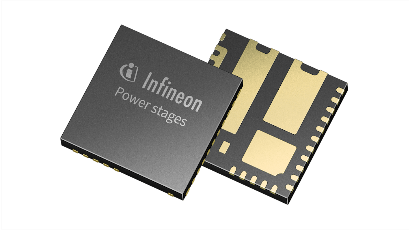
The Infineon TDA21472 power stage contains a low quiescent-current synchronous buck gate-driver IC co-packaged with Schottky diode, and high-side and low-side MOSFETs. The package is optimized for PCB layout, heat transfer, driver/MOSFET control timing, and minimal switch node ringing when layout guidelines are followed. The gate driver and MOSFET combination enables higher efficiency at the lower output voltages required by cutting edge CPU, GPU and DDR memory designs.
Thermal shutdown and fault flag
Cycle-by-cycle over current protection with programmable threshold and fault flag
MOSFET phase fault detection and flag
Auto-replenishment of bootstrap capacitor
Deep-sleep mode for power saving
Compatible with 3.3-V tri-state PWM input
Body-Braking load transient support