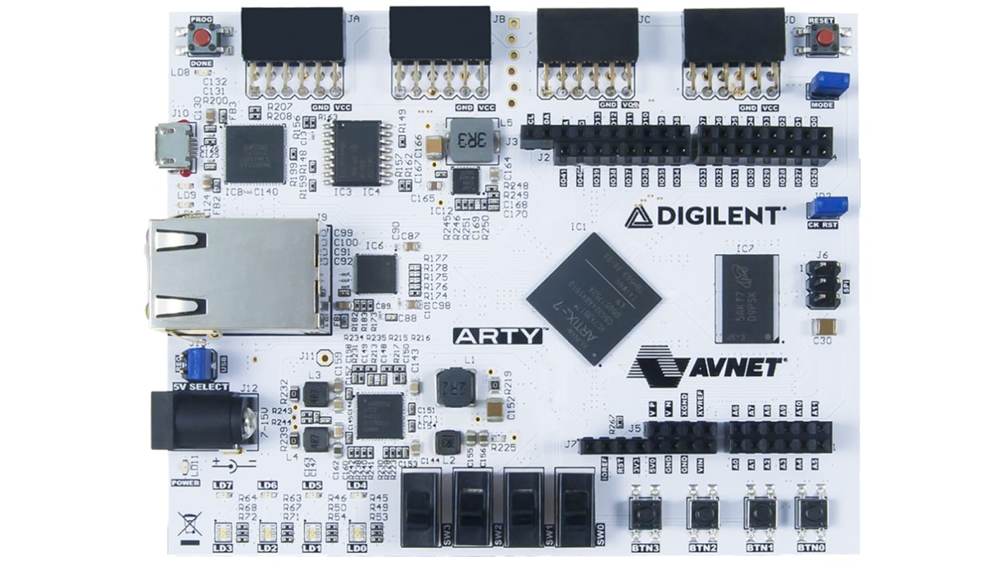
Digilent 410-319 Arty Artix-7 Development Board

Currently unavailable
We don't know if this item will be back in stock, RS intend to remove it from our range soon.
RS Stock No.:
134-6478
Mfr. Part No.:
410-319
Brand:
Digilent
Find similar products by selecting one or more attributes.
Select all

Brand

Digilent

Programmable Logic Technology

FPGA

Kit Classification

Development Board

Kit Name

Arty Artix-7

Arty Artix-7 FPGA Development Board


Arty is a development platform designed around the Artix-7™ Field Programmable Gate Array (FPGA) from Xilinx. Arty was designed specifically for use as a MicroBlaze Soft Processing System.

Xilinx Artix-7 FPGA (XC7A35T-1CSG324-1L)


• 33280 logic cells in 5200 slices (each slice contains 4 x 6-input LUTs and 8 x flip-flops)
• 1800Kbit Fast Block RAM
• 5 x Clock Management Tiles, each with a phase-locked loop (PLL)
• 90 x DSP slices
• Internal clock speeds exceeding 450MHz
• On-chip Analogue-to-Digital Converter (XADC)
• Programmable over JTAG and Quad-SPI Flash

Board Memory and Power


• 256MB DDR3L SDRAM with 16-bit bus @ 667MHz
• 16MB Quad-SPI Flash memory
• USB-JTAG Programming circuit
• Powered from USB connector or +7V to +15Vdc barrel jack socket

System Connectivity


• 10/100 Ethernet via RJ45 connector
• USB-UART Bridge via microUSB socket

Switches and LEDs


• 4 x User Slide-Switches
• 4 x User Pushbuttons
• Reset Pushbutton
• Status LEDs: Power-on, FPGA programming status and USB/Ethernet port status
• 4 x User LEDs
• 4 x User RGB LEDs

Expansion Connectors


• 2 x Standard Pmod™ 2 x 6-pin connectors
• 2 x High-Speed Pmod™ 2 x 6-pin connectors
• chipKIT/Arduino R3 Shield headers

Note

An adapter Shield allowing up to five more Pmod™ peripheral modules to be interfaced is available: RS 136-8283
Software Voucher Code is provided on the product packaging


An FPGA is a semiconductor device consisting of a matrix of Configurable Logic Blocks (CLBs) connected through programmable interconnects. The user determines these interconnections by programming SRAM. A CLB can be simple (AND, OR gates, etc) or complex (a block of RAM). The FPGA allows changes to be made to a design even after the device is soldered into a PCB.