Digilent 410-316 Nexys Video Artix-7 Development Board ADC1410 for DAC121S101
- RS Stock No.:
- 134-6477
- Distrelec Article No.:
- 300-44-277
- Mfr. Part No.:
- 410-316
- Brand:
- Digilent

Subtotal (1 unit)*
£435.75
(exc. VAT)
£522.90
(inc. VAT)
FREE delivery for orders over £60.00
Temporarily out of stock
- 1 unit(s) shipping from 30 July 2026
- Plus 3 unit(s) shipping from 20 August 2026
- Plus 8 unit(s) shipping from 27 August 2026
Need more? Click ‘Check delivery dates’ to find extra stock and lead times.
Units | Per unit |
|---|---|
| 1 + | £435.75 |
*price indicative
- RS Stock No.:
- 134-6477
- Distrelec Article No.:
- 300-44-277
- Mfr. Part No.:
- 410-316
- Brand:
- Digilent
Specifications
Technical Reference
Legislation and Compliance
Product Details
Find similar products by selecting one or more attributes.
Select all | Attribute | Value |
|---|---|---|
| Brand | Digilent | |
| Product Type | Programmable Logic Development Kit | |
| Kit Classification | Development Board | |
| Programmable Logic Technology | FPGA | |
| For Use With | DAC121S101 | |
| Featured Device | ADC1410 | |
| Kit Name | Nexys Video Artix-7 | |
| Standards/Approvals | RoHS | |
| Select all | ||
|---|---|---|
Brand Digilent | ||
Product Type Programmable Logic Development Kit | ||
Kit Classification Development Board | ||
Programmable Logic Technology FPGA | ||
For Use With DAC121S101 | ||
Featured Device ADC1410 | ||
Kit Name Nexys Video Artix-7 | ||
Standards/Approvals RoHS | ||
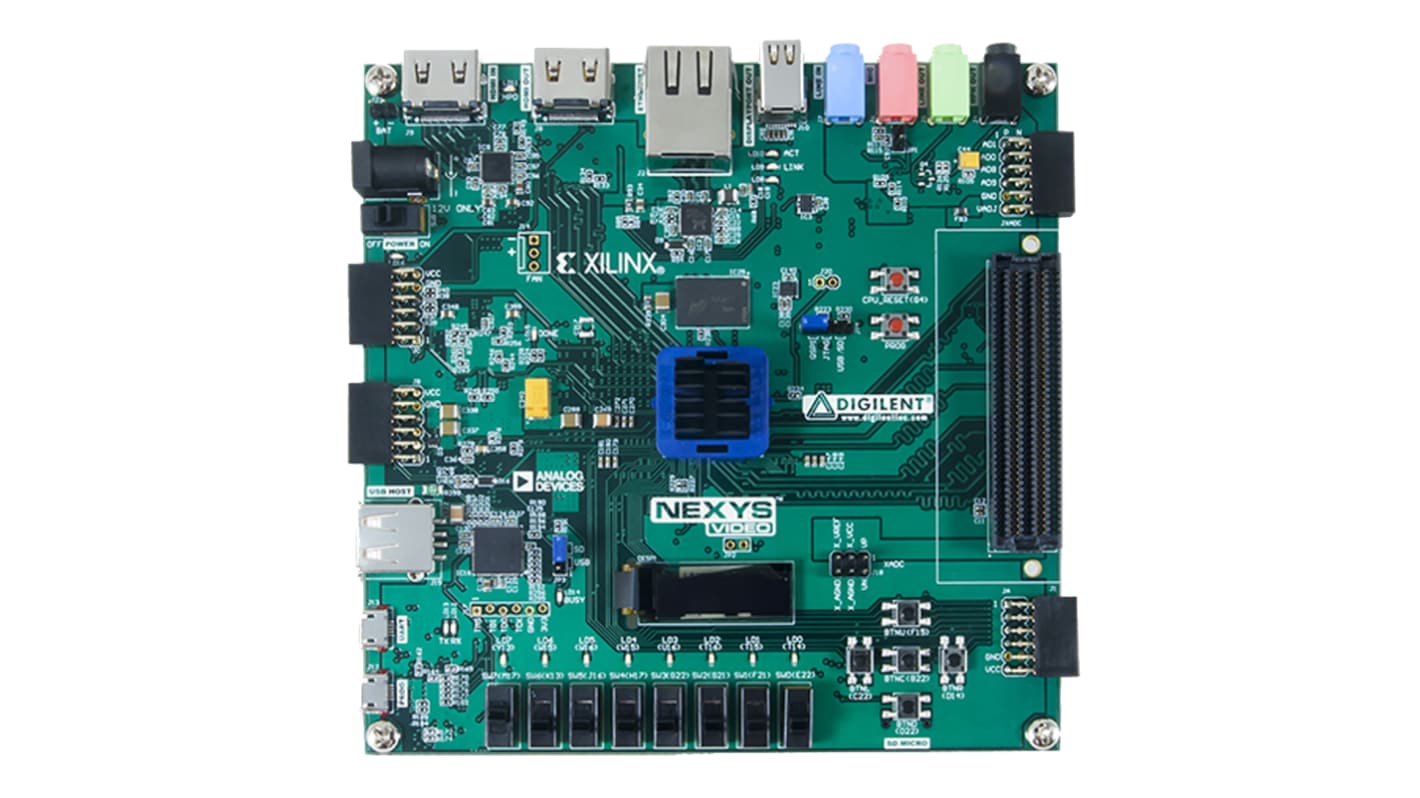
Nexys Video Artix-7 FPGA Trainer Board
The Nexys Video FPGA Board features a large, high-capacity Artix-7 FPGA device, generous external memories, high-speed digital video ports and a 24-bit audio codec. It is perfectly suited for audio and video processing applications. Compatible with ISE® toolset and the Vivado® Design Suite. It is also supported under the free WebPACK™ license.
Xilinx Artix-7 FPGA (XC7A200T-1SBG484C) Features
• 215360 logic cells in 33650 slices (each slice contains 4 x 6-input LUTs and 8 x flip-flops)
• 13Mbit Fast Block RAM
• 10 x Clock Management Tiles, each with a phase-locked loop (PLL)
• 740 x DSP slices
• Internal clock speeds exceeding 450MHz
• On-chip Analogue-to-Digital Converter (XADC)
• Up to 3.75Gbps GTP transceivers
Nexys Video Board Features
• MT41K256M16HA-187E 512MiB DDR3 SDRAM
• S25FL256S 32MiB Quad-SPI Serial Flash memory
• 24AA025E48 EEPROM for Ethernet node MAC address
• ADAU1761 SigmaDSP stereo audio codec
• HDMI output connector
• HDMI input connector
• Programmable over JTAG, Quad-SPI or USB
• 0.91in 128 x 32pixel OLED display
• FPGA Programming-Done LED
• 8 x User LEDs
• 5 x User Pushbuttons
• 8 x User Slide-Switches
• MicroUSB (JTAG) connector for USB programming
• USB-UART Bridge via microUSB socket
• USB-A HID Host socket for mice, keyboards and memory sticks
• DisplayPort output mDP connector
• 160-pin LPC FMC connector
• RJ45 socket for 10/100/1000 Ethernet connection
• 3.5mm jack socket for mono microphone In
• 3.5mm jack socket for stereo audio Line In
• 3.5mm jack socket for stereo audio Line Out
• 3.5mm jack socket for stereo headphone Out
• microSD card slot
• 3 x Standard Pmod 2 x 6-pin connectors
• Dual Analogue/Digital XADC Pmod 2 x 6-pin connector
• Powered from barrel jack socket or external +12Vdc header
An FPGA is a semiconductor device consisting of a matrix of Configurable Logic Blocks (CLBs) connected through programmable interconnects. The user determines these interconnections by programming SRAM. A CLB can be simple (AND, OR gates, etc) or complex (a block of RAM). The FPGA allows changes to be made to a design even after the device is soldered into a PCB.
Supplied with
Hardshell plastic case with protective foam, USB cable
Related links
- Digilent 410-292 Nexys A7-100T Nexys 4 DDR Artix-7 Development Board ADC1410 for DAC121S101
- Digilent 410-183 Basys Artix-7 Development Board ADC1410 for DAC121S101
- Digilent 410-300 GENESYS2 KINTEX-7 Development Board ADC1410 for DAC121S101
- Digilent 410-328-35 Cmod A7 Artix-7 Module ADC1410 for DAC121S101
- Digilent 410-319-1 FPGA Development Board for Makers and Hobbyists Development Board ADC1410 for DAC121S101
- Digilent 410-376 Xilinx Spartan-7 Development Board ADC1410 for XC7S25 Spartan-7
- Digilent 410-352 Xilinx Spartan-7 Development Board ADC1410 for Hobbyists Makers
- Digilent 410-370 Cora Z7: Zynq-7000 Development Board ADC1410 for FPGA Development, ARM Development