Cypress Semiconductor NOR 32Mbit CFI Flash Memory 48-Pin BGA, S29JL032J70BHI320
- RS Stock No.:
- 193-8917
- Mfr. Part No.:
- S29JL032J70BHI320
- Brand:
- Cypress Semiconductor

Unavailable
RS will no longer stock this product.
- RS Stock No.:
- 193-8917
- Mfr. Part No.:
- S29JL032J70BHI320
- Brand:
- Cypress Semiconductor
Specifications
Technical Reference
Legislation and Compliance
Product Details
Find similar products by selecting one or more attributes.
Select all | Attribute | Value |
|---|---|---|
| Brand | Cypress Semiconductor | |
| Memory Size | 32Mbit | |
| Interface Type | CFI | |
| Package Type | BGA | |
| Pin Count | 48 | |
| Organisation | 4M x 8 bit | |
| Mounting Type | Surface Mount | |
| Cell Type | NOR | |
| Minimum Operating Supply Voltage | 2.7 V | |
| Maximum Operating Supply Voltage | 3.6 V | |
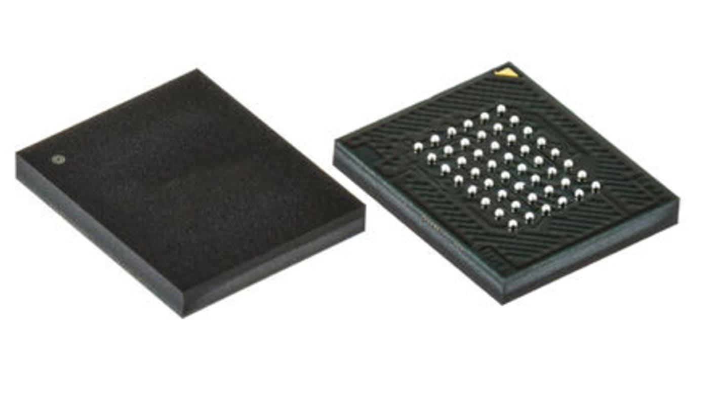
| Dimensions | 8.15 x 6.15 x 0.84mm | |
| Maximum Random Access Time | 70ns | |
| Maximum Operating Temperature | +85 °C | |
| Number of Bits per Word | 8bit | |
| Minimum Operating Temperature | -40 °C | |
| Number of Words | 4M | |
| Number of Banks | 4 | |
| Select all | ||
|---|---|---|
Brand Cypress Semiconductor | ||
Memory Size 32Mbit | ||
Interface Type CFI | ||
Package Type BGA | ||
Pin Count 48 | ||
Organisation 4M x 8 bit | ||
Mounting Type Surface Mount | ||
Cell Type NOR | ||
Minimum Operating Supply Voltage 2.7 V | ||
Maximum Operating Supply Voltage 3.6 V | ||
Dimensions 8.15 x 6.15 x 0.84mm | ||
Maximum Random Access Time 70ns | ||
Maximum Operating Temperature +85 °C | ||
Number of Bits per Word 8bit | ||
Minimum Operating Temperature -40 °C | ||
Number of Words 4M | ||
Number of Banks 4 | ||
The S29JL032J is a 32 Mb, 3.0 volt-only flash memory device, organized as 2,097,152 words of 16 bits each or 4,194,304 bytes of 8 bits each. Word mode data appears on DQ15–DQ0, byte mode data appears on DQ7–DQ0. The device is designed to be programmed in-system with the standard 3.0 volt VCC supply and can also be programmed in standard EPROM programmers. The device is available with an access time of 60, or 70 ns and is offered in a 48-ball FBGA or a 48pin TSOP package. Standard control pins chip enable (CE#), write enable (WE#) and output enable (OE#) control normal read and write operations and avoid bus contention issues. The device requires only a single 3.0 volt power supply for both read and write functions. Internally generated and regulated voltages are provided for the program and erase operations.