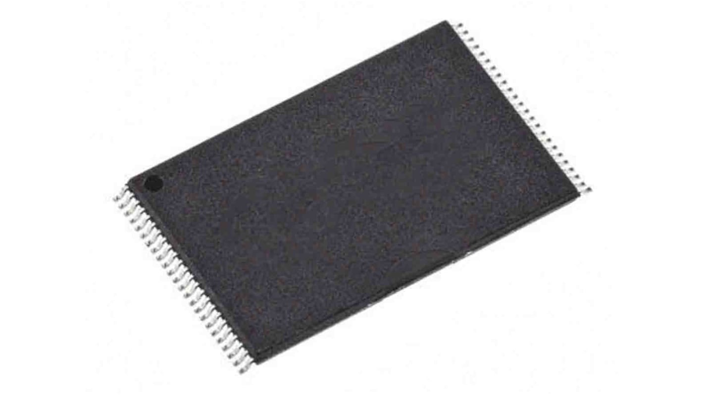
Infineon NOR 16 MB CFI Flash Memory 48-Pin TSOP
- RS Stock No.:
- 193-8787P
- Mfr. Part No.:
- S29AL016J70TFI013
- Brand:
- Infineon

Currently unavailable
We don't know if this item will be back in stock, RS intend to remove it from our range soon.
- RS Stock No.:
- 193-8787P
- Mfr. Part No.:
- S29AL016J70TFI013
- Brand:
- Infineon
Specifications
Technical Reference
Legislation and Compliance
Product Details
Find similar products by selecting one or more attributes.
Select all | Attribute | Value |
|---|---|---|
| Brand | Infineon | |
| Product Type | Flash Memory | |
| Memory Size | 16MB | |
| Interface Type | CFI | |
| Package Type | TSOP | |
| Pin Count | 48 | |
| Organisation | 2M x 8 bit | |
| Mount Type | Surface | |
| Cell Type | NOR | |
| Maximum Supply Voltage | 3.6V | |
| Minimum Supply Voltage | 2.7V | |
| Timing Type | Asynchronous | |
| Minimum Operating Temperature | -40°C | |
| Maximum Operating Temperature | 85°C | |
| Length | 12mm | |
| Standards/Approvals | No | |
| Width | 12mm | |
| Height | 1.05mm | |
| Supply Current | 12mA | |
| Series | S29AL016J | |
| Number of Bits per Word | 8 | |
| Maximum Random Access Time | 70ns | |
| Automotive Standard | AEC-Q100 | |
| Number of Words | 2M | |
| Select all | ||
|---|---|---|
Brand Infineon | ||
Product Type Flash Memory | ||
Memory Size 16MB | ||
Interface Type CFI | ||
Package Type TSOP | ||
Pin Count 48 | ||
Organisation 2M x 8 bit | ||
Mount Type Surface | ||
Cell Type NOR | ||
Maximum Supply Voltage 3.6V | ||
Minimum Supply Voltage 2.7V | ||
Timing Type Asynchronous | ||
Minimum Operating Temperature -40°C | ||
Maximum Operating Temperature 85°C | ||
Length 12mm | ||
Standards/Approvals No | ||
Width 12mm | ||
Height 1.05mm | ||
Supply Current 12mA | ||
Series S29AL016J | ||
Number of Bits per Word 8 | ||
Maximum Random Access Time 70ns | ||
Automotive Standard AEC-Q100 | ||
Number of Words 2M | ||
The S29AL016J is a 16 Mbit, 3.0 Volt-only Flash memory organized as 2,097,152 bytes or 1,048,576 words. The device is offered in 48-ball Fine-pitch BGA (0.8 mm pitch), 64-ball Fortified BGA (1.0 mm pitch) and 48pin TSOP packages. The word-wide data (x16)appears on DQ15–DQ0, the byte-wide (x8) data appears on DQ7–DQ0. This device is designed to be programmed in-system with the standard system 3.0 volt VCC supply. A 12.0 V VPP or 5.0 VCC are not required for write or erase operations. The device can also be programmed in standard EPROM programmers.
The device offers access time of 55 ns allowing high speed microprocessors to operate without wait states. To eliminate bus contention the device has separate chip enable (CE#), write enable (WE#) and output enable (OE#) controls.
Device programming occurs by executing the program command sequence. This initiates the Embedded Program algorithm an internal algorithm that automatically times the program pulse widths and verifies proper cell margin. The Unlock Bypass mode facilitates faster programming times by requiring only two write cycles to program data instead of four.
Device erasure occurs by executing the erase command sequence. This initiates the Embedded Erase algorithm an internal algorithm that automatically preprograms the array (if it is not already programmed) before executing the erase operation. During erase, the device automatically times the erase pulse widths and verifies proper cell margin. The host system can detect whether a program or erase operation is complete by observing the RY/BY# pin, or by reading the DQ7(Data# Polling) and DQ6 (toggle) status bits. After a program or erase cycle has been completed, the device is ready to read array data or accept another command.