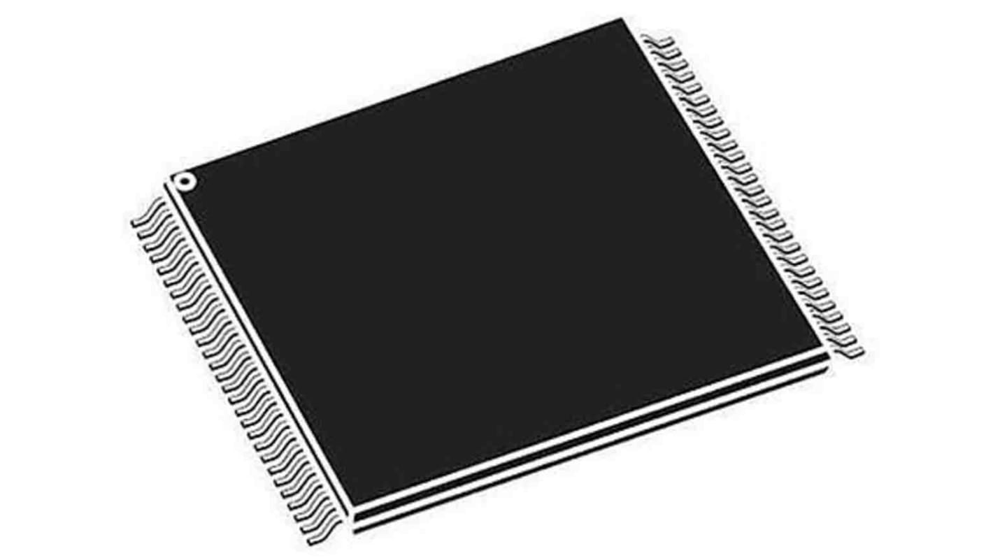
Cypress Semiconductor NOR 512Mbit CFI Flash Memory 56-Pin TSOP, S29GL512T10TFI020
- RS Stock No.:
- 182-3370P
- Mfr. Part No.:
- S29GL512T10TFI020
- Brand:
- Cypress Semiconductor

Bulk discount available
Subtotal 10 units (supplied in a tray)*
£62.50
(exc. VAT)
£75.00
(inc. VAT)
Stock information currently inaccessible - Please check back later
Units | Per unit |
|---|---|
| 10 - 24 | £6.25 |
| 25 - 49 | £5.70 |
| 50 - 99 | £5.40 |
| 100 + | £5.17 |
*price indicative
- RS Stock No.:
- 182-3370P
- Mfr. Part No.:
- S29GL512T10TFI020
- Brand:
- Cypress Semiconductor
Specifications
Technical Reference
Legislation and Compliance
Product Details
Find similar products by selecting one or more attributes.
Select all | Attribute | Value |
|---|---|---|
| Brand | Cypress Semiconductor | |
| Memory Size | 512Mbit | |
| Interface Type | CFI | |
| Package Type | TSOP | |
| Pin Count | 56 | |
| Organisation | 64M x 8 bit | |
| Mounting Type | Surface Mount | |
| Cell Type | NOR | |
| Minimum Operating Supply Voltage | 2.7 V | |
| Maximum Operating Supply Voltage | 3.6 V | |
| Dimensions | 18.5 x 14.1 x 1.05mm | |
| Minimum Operating Temperature | -40 °C | |
| Number of Words | 64M | |
| Maximum Operating Temperature | +85 °C | |
| Number of Bits per Word | 8bit | |
| Maximum Random Access Time | 100ns | |
| Select all | ||
|---|---|---|
Brand Cypress Semiconductor | ||
Memory Size 512Mbit | ||
Interface Type CFI | ||
Package Type TSOP | ||
Pin Count 56 | ||
Organisation 64M x 8 bit | ||
Mounting Type Surface Mount | ||
Cell Type NOR | ||
Minimum Operating Supply Voltage 2.7 V | ||
Maximum Operating Supply Voltage 3.6 V | ||
Dimensions 18.5 x 14.1 x 1.05mm | ||
Minimum Operating Temperature -40 °C | ||
Number of Words 64M | ||
Maximum Operating Temperature +85 °C | ||
Number of Bits per Word 8bit | ||
Maximum Random Access Time 100ns | ||
- COO (Country of Origin):
- US
48 nm MirrorBit Eclipse Technology
Single supply (VCC) for read / program / erase (2.7 V to 3.6 V)
Versatile I/O feature
Wide I/O voltage range (VIO): 1.65 V to VCC
x8/x16 data bus
Asynchronous 32-byte Page read
512-byte Programming Buffer
Programming in ltiples, up to a maximum of 512 bytes
Single word and multiple program on same word options
Automatic Error Checking and Correction (ECC) — internal hardware ECC with single bit error correction
Sector Erase
Uniform 128-KB sectors
Suspend and Resume commands for Program and Erase operations
Status Register, Data Polling, and Ready/Busy pin methods to determine device status
Advanced Sector Protection (ASP)
Volatile and non-volatile protection methods for each sector
Separate 2048-byte One-Time Program (OTP) array
Four lockable regions (SSR0 - SSR3)
SSR0 is Factory Locked
SSR3 is Password Read Protect
Common Flash Interface (CFI) parameter table
Temperature Range / Grade:
Industrial (-40°C to +85°C)
Industrial Plus (-40°C to +105°C)
Extended (-40°C to +125°C)
100,000 Program / Erase Cycles
20-year data retention
Packaging Options
56-pin TSOP
64-ball LAA Fortified BGA, 13 mm x 11 mm
64-ball LAE Fortified BGA, 9 mm x 9 mm
56-ball VBU Fortified BGA, 9 mm x 7 mm