Digilent 410-249 Programming Adapter for use with Xilinx FPGAs
- RS Stock No.:
- 134-6458
- Distrelec Article No.:
- 300-44-264
- Mfr. Part No.:
- 410-249
- Brand:
- Digilent

Bulk discount available
Subtotal (1 unit)*
£52.73
(exc. VAT)
£63.28
(inc. VAT)
FREE delivery for orders over £60.00
In Stock
- 16 unit(s) ready to ship
- Plus 4 unit(s) ready to ship from another location
- Plus 6 unit(s) shipping from 15 May 2026
Need more? Click ‘Check delivery dates’ to find extra stock and lead times.
Units | Per unit |
|---|---|
| 1 - 4 | £52.73 |
| 5 - 9 | £50.09 |
| 10 + | £48.50 |
*price indicative
- RS Stock No.:
- 134-6458
- Distrelec Article No.:
- 300-44-264
- Mfr. Part No.:
- 410-249
- Brand:
- Digilent
Specifications
Technical Reference
Legislation and Compliance
Product Details
Find similar products by selecting one or more attributes.
Select all | Attribute | Value |
|---|---|---|
| Brand | Digilent | |
| Product Type | Development Kit Accessory | |
| Accessory Type | Programming Adapter | |
| For Use With | Xilinx FPGAs | |
| Standards/Approvals | No | |
| Select all | ||
|---|---|---|
Brand Digilent | ||
Product Type Development Kit Accessory | ||
Accessory Type Programming Adapter | ||
For Use With Xilinx FPGAs | ||
Standards/Approvals No | ||
- COO (Country of Origin):
- TW
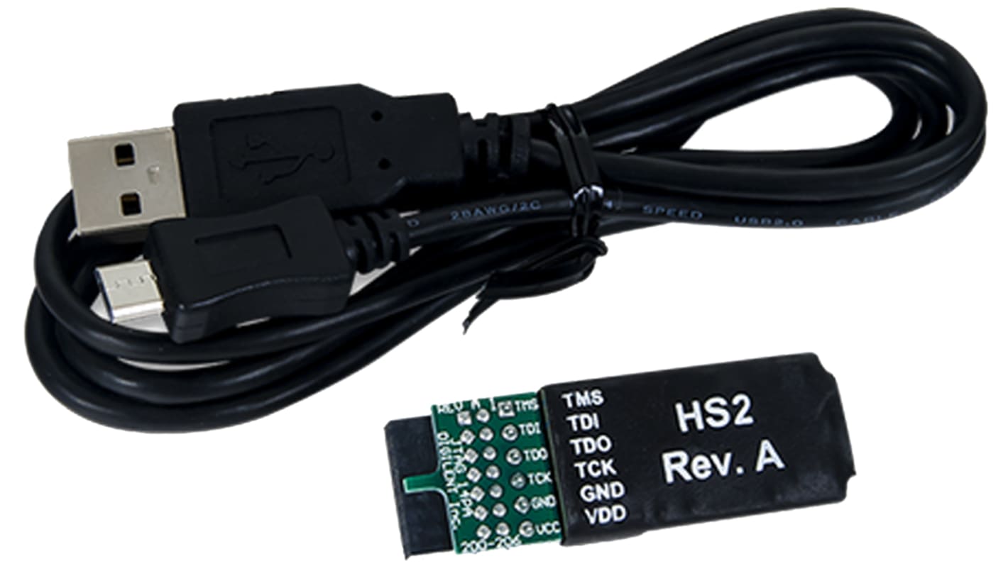
JTAG-HS2 FPGA Programming Cable
The JTAG-HS2 programming cable allows high-speed programming of Xilinx FPGA devices from a host PC.
Features
• Compatible with all Xilinx tools
• Compatible with IEEE 1149.7-2009 Class T0 - Class T4 (includes 2-Wire JTAG)
• On-board ADP123AUJZ 300mA voltage regulator
• Separate Vref drives JTAG/SPI signal voltages
• Vref can be any voltage between +1.8V and +5V
• USB 2.0 HS port drives JTAG/SPI bus at up to 30Mbit/sec
• JTAG/SPI frequency settable by user
• PC connector: MicroUSB
• JTAG connector: 0.1in 6-pin
• SPI programming modes 0/2 up to 30Mbit/sec, modes 1/3 up to 2Mbit/sec
• Fully supported by Digilent's Adept software and Adept SDK
Supported Target Devices
• Xilinx FPGAs
• Xilinx Zynq-7000
• Xilinx CoolRunner™/CoolRunner-II CPLDs
• Xilinx Platform Flash ISP configuration PROMs
• Selected third-party SPI PROMs
• Selected third-party BPI PROMs
Target Devices Not Supported
• Xilinx 9500/9500XL CPLDs
• Xilinx 1700 and 18V00 ISP configuration PROMs
• Xilinx FPGA eFUSE programming
An FPGA is a semiconductor device consisting of a matrix of Configurable Logic Blocks (CLBs) connected through programmable interconnects. The user determines these interconnections by programming SRAM. A CLB can be simple (AND, OR gates, etc) or complex (a block of RAM). The FPGA allows changes to be made to a design even after the device is soldered into a PCB.
Note
This cable is not needed for Digilent Xilinx FPGA boards as they have this functionality built-in.
Supplied with
Xilinx JTAG 2 x 7-pin 2mm connector adapter, USB cable
Related links
- Digilent 410-299 Programming Cable for use with Xilinx Tool, JTAG-HS3
- Digilent 410-308 Programming Module for use with FPGA Devices
- Digilent 410-251 Programming Module for use with FPGA Devices
- Digilent 410-361 Adapter
- Digilent 410-372 Adapter for use with APSoC Development Board, FPGA
- Digilent 410-413 Transistor Tester Adapter for use with Analog Discovery 2 and Analog Discovery (Legacy)
- Digilent 410-373 Breadboard for use with Breadboard
- Digilent 410-384 for use with Breadboard