Nexperia 74HC597D,653 1 Surface Shift Register 74HC SO, 16-Pin
- RS Stock No.:
- 170-8019
- Mfr. Part No.:
- 74HC597D,653
- Brand:
- Nexperia

Subtotal (1 reel of 2500 units)*
£410.00
(exc. VAT)
£492.50
(inc. VAT)
FREE delivery for orders over £60.00
Temporarily out of stock
- Shipping from 03 September 2026
Need more? Click ‘Check delivery dates’ to find extra stock and lead times.
Units | Per unit | Per Reel* |
|---|---|---|
| 2500 + | £0.164 | £410.00 |
*price indicative
- RS Stock No.:
- 170-8019
- Mfr. Part No.:
- 74HC597D,653
- Brand:
- Nexperia
Specifications
Technical Reference
Legislation and Compliance
Product Details
Find similar products by selecting one or more attributes.
Select all | Attribute | Value |
|---|---|---|
| Brand | Nexperia | |
| Product Type | Shift Register | |
| Package Type | SO | |
| Logic Family | 74HC | |
| Mount Type | Surface | |
| Number of Elements | 1 | |
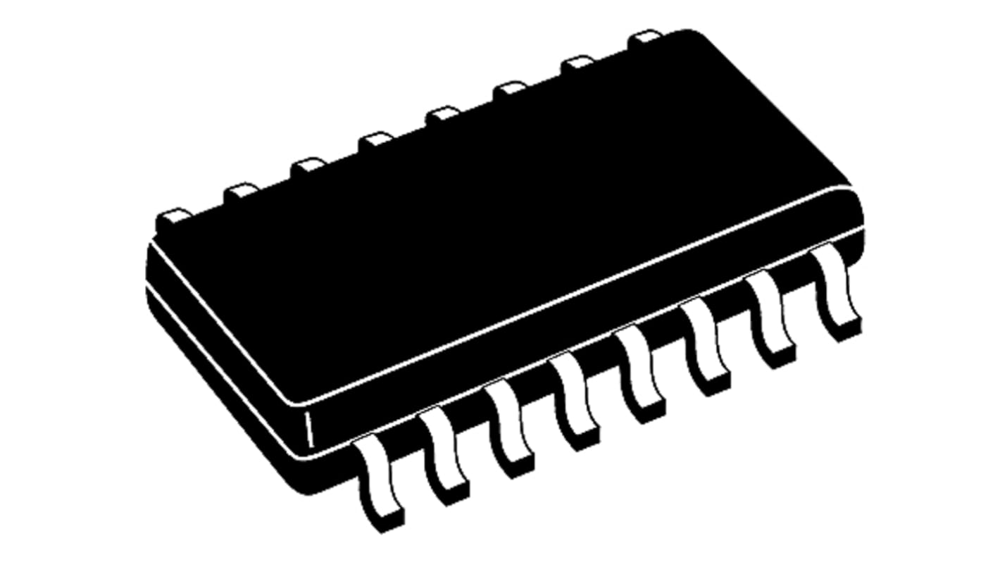
| Pin Count | 16 | |
| Minimum Supply Voltage | 2V | |
| Maximum Supply Voltage | 6V | |
| Trigger Type | Positive Edge | |
| Maximum Operating Temperature | 125°C | |
| Height | 1.75mm | |
| Series | 74HC597 | |
| Standards/Approvals | No | |
| Length | 10mm | |
| Automotive Standard | No | |
| Select all | ||
|---|---|---|
Brand Nexperia | ||
Product Type Shift Register | ||
Package Type SO | ||
Logic Family 74HC | ||
Mount Type Surface | ||
Number of Elements 1 | ||
Pin Count 16 | ||
Minimum Supply Voltage 2V | ||
Maximum Supply Voltage 6V | ||
Trigger Type Positive Edge | ||
Maximum Operating Temperature 125°C | ||
Height 1.75mm | ||
Series 74HC597 | ||
Standards/Approvals No | ||
Length 10mm | ||
Automotive Standard No | ||
The 74HC595, 74HCT595 is an 8-bit serial-in/serial or parallel-out shift register with a storage register and 3-state outputs. Both the shift and storage register have separate clocks. The device features a serial input (DS) and a serial output (Q7S) to enable cascading and an asynchronous reset MR input. A LOW on MR will reset the shift register. Data is shifted on the LOW-to-HIGH transitions of the SHCP input. The data in the shift register is transferred to the storage register on a LOW-to-HIGH transition of the STCP input. If both clocks are connected together, the shift register will always be one clock pulse ahead of the storage register.
Simple control interface
I/O expansion
Asynchronous and synchronous load options
High frequency
Cascadable
LED drivers
Key applications
Displays
Control units