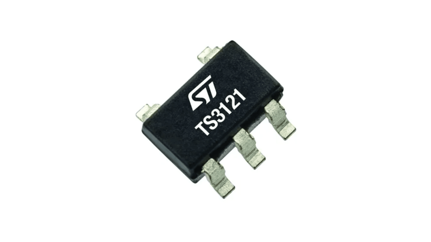
TS3121IYLT STMicroelectronics 1-Channel Comparator Open Drain O/P, 5.5 V 1.7 V 5-Pin SOT-323-5
- RS Stock No.:
- 285-644
- Mfr. Part No.:
- TS3121IYLT
- Brand:
- STMicroelectronics

Bulk discount available
Subtotal (1 unit)*
£1.24
(exc. VAT)
£1.49
(inc. VAT)
FREE delivery for orders over £60.00
In Stock
- 3,000 unit(s) ready to ship
Need more? Click ‘Check delivery dates’ to find extra stock and lead times.
Units | Per unit |
|---|---|
| 1 - 9 | £1.24 |
| 10 - 99 | £1.13 |
| 100 - 499 | £1.04 |
| 500 - 999 | £0.95 |
| 1000 + | £0.85 |
*price indicative
- RS Stock No.:
- 285-644
- Mfr. Part No.:
- TS3121IYLT
- Brand:
- STMicroelectronics
Specifications
Technical Reference
Legislation and Compliance
Product Details
Find similar products by selecting one or more attributes.
Select all | Attribute | Value |
|---|---|---|
| Brand | STMicroelectronics | |
| Comparator Type | Analogue Comparator | |
| Product Type | Comparator | |
| Mount Type | Surface | |
| Package Type | SOT-323-5 | |
| Output Type | Open Drain | |
| Number of Channels | 1 | |
| Pin Count | 5 | |
| Maximum Supply Voltage | 5.5V | |
| Minimum Supply Voltage | 1.7V | |
| Minimum Operating Temperature | -40°C | |
| Maximum Operating Temperature | 125°C | |
| Height | 1.6mm | |
| Length | 2.9mm | |
| Standards/Approvals | AEC-Q100 | |
| Series | TS | |
| Automotive Standard | AEC-Q100 | |
| Supply Current | 125μA | |
| Select all | ||
|---|---|---|
Brand STMicroelectronics | ||
Comparator Type Analogue Comparator | ||
Product Type Comparator | ||
Mount Type Surface | ||
Package Type SOT-323-5 | ||
Output Type Open Drain | ||
Number of Channels 1 | ||
Pin Count 5 | ||
Maximum Supply Voltage 5.5V | ||
Minimum Supply Voltage 1.7V | ||
Minimum Operating Temperature -40°C | ||
Maximum Operating Temperature 125°C | ||
Height 1.6mm | ||
Length 2.9mm | ||
Standards/Approvals AEC-Q100 | ||
Series TS | ||
Automotive Standard AEC-Q100 | ||
Supply Current 125μA | ||
- COO (Country of Origin):
- MY
The STMicroelectronics TS3121 single comparators permit high-speed response time at low power consumption over a supply voltage specified from 1.7 to 5.5 V. These devices operate over a wide temperature range from -40 °C to +125 °C making them Ideal for industrial and automotive applications with the associated qualification. Thanks to an embedded fail-safe circuit, the TS3121 and the TS3121A can operate with input/output pins biased while the supply pin is shut down to VCC = 0 V for energy saving applications. A guaranteed start-up time ensures a stable output condition after activating the supply rail. Thanks to their small package size, the TS3121 and the TS3121A can be used in applications where space on the board is limited. It can thus reduce the overall cost of the PCB.
Low offset voltage 2mV max 25°C for A-grade version
Low power consumption 70 μA typ
Wide supply voltage 1.7 to 5.5 V
Propagation delay 60 ns
Fail-safe input and output pins
Input and output pins withstand voltages higher than VCC
Fail safe architecture keeps output in high impedance when VCC = 0 V
Guaranteed start-up time allows sequential on and off cycles of VCC
High ESD tolerance 4 kV HBM
Related links
- TS3121IYLT STMicroelectronics 1-Channel Comparator Open Drain O/P, 5.5 V 1.7 V 5-Pin SOT-323-5
- TS3121ILT STMicroelectronics 1-Channel Comparator Open Drain O/P, 60 ns 5.5 V 1.7 V 5-Pin SOT-323-5
- TS3121AIYLT STMicroelectronics 1-Channel Comparator Open Drain O/P, 60 ns 5.5 V 1.7 V 5-Pin SOT-23-5
- TS3121AILT STMicroelectronics 1-Channel Comparator Open Drain O/P, 60 ns 5.5 V 1.7 V 5-Pin SOT-23-5
- TS3121ICT STMicroelectronics 1-Channel Comparator Open Drain O/P, 60 ns 5.5 V 1.7 V 5-Pin SOT-23-5
- TS3121AICT STMicroelectronics 1-Channel Comparator Open Drain O/P, 60 ns 5.5 V 1.7 V 5-Pin SC-70-5
- TS3121AIYCT STMicroelectronics 1-Channel Comparator Open Drain O/P, 60 ns 5.5 V 1.7 V 5-Pin SC-70-5
- TS3121IYCT STMicroelectronics 1-Channel Comparator Open Drain O/P, 60 ns 5.5 V 1.7 V 5-Pin SC-70-5
