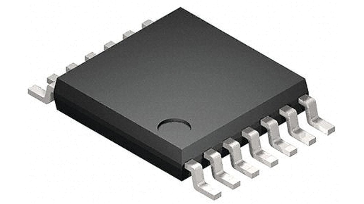
Toshiba 74VHCT126AFT Non-Inverting 3 State Octal Bus Buffer, 14-Pin TSSOP
- RS Stock No.:
- 171-3560P
- Mfr. Part No.:
- 74VHCT126AFT
- Brand:
- Toshiba

Currently unavailable
We don't know if this item will be back in stock, RS intend to remove it from our range soon.
- RS Stock No.:
- 171-3560P
- Mfr. Part No.:
- 74VHCT126AFT
- Brand:
- Toshiba
Specifications
Technical Reference
Legislation and Compliance
Product Details
Find similar products by selecting one or more attributes.
Select all | Attribute | Value |
|---|---|---|
| Brand | Toshiba | |
| Product Type | Octal Bus Buffer | |
| Logic Family | 74VHCT | |
| Logic Function | Buffer | |
| Schmitt Trigger Input | No | |
| Input Type | CMOS | |
| Output Type | 3 State | |
| Mount Type | Surface | |
| Polarity | Non-Inverting | |
| Package Type | TSSOP | |
| Minimum Supply Voltage | 4.5V | |
| Pin Count | 14 | |
| Maximum Supply Voltage | 5.5V | |
| Maximum High Level Output Current | -8mA | |
| Maximum Propagation Delay Time @ CL | 3.8ns | |
| Minimum Operating Temperature | -40°C | |
| Maximum Low Level Output Current | 8mA | |
| Maximum Operating Temperature | 125°C | |
| Length | 5mm | |
| Standards/Approvals | No | |
| Height | 1mm | |
| Width | 4.4 mm | |
| Supply Current | 4μA | |
| Automotive Standard | AEC-Q100 | |
| Select all | ||
|---|---|---|
Brand Toshiba | ||
Product Type Octal Bus Buffer | ||
Logic Family 74VHCT | ||
Logic Function Buffer | ||
Schmitt Trigger Input No | ||
Input Type CMOS | ||
Output Type 3 State | ||
Mount Type Surface | ||
Polarity Non-Inverting | ||
Package Type TSSOP | ||
Minimum Supply Voltage 4.5V | ||
Pin Count 14 | ||
Maximum Supply Voltage 5.5V | ||
Maximum High Level Output Current -8mA | ||
Maximum Propagation Delay Time @ CL 3.8ns | ||
Minimum Operating Temperature -40°C | ||
Maximum Low Level Output Current 8mA | ||
Maximum Operating Temperature 125°C | ||
Length 5mm | ||
Standards/Approvals No | ||
Height 1mm | ||
Width 4.4 mm | ||
Supply Current 4μA | ||
Automotive Standard AEC-Q100 | ||
The 74VHCT125AFT and 74VHCT126AFT are high speed CMOS QUAD BUS BUFFERs fabricated with silicon gate C2MOS technology. They achieve the high speed operation similar to equivalent Bipolar Schottky TTL while maintaining the CMOS low power dissipation. The 74VHCT125AFT requires the 3-state control input G to be set high to place the output into the high impedance state, whereas the 74VHCT126AFT requires the control input G to be set low to place the output into high impedance. The input voltage are compatible with TTL output voltage. This device may be used as a level converter for interfacing 3.3 V to 5 V system. Input protection and output circuit ensure that 0 to 5.5 V can be applied to the input and output (Note) pins without regard to the supply voltage. There structure prevents device destruction due to mismatched supply and input/output voltages such as battery back up, hot board insertion, etc.
Wide operating temperature range: Topr = -40 to 125
High speed: Propagation delay time = 3.8 ns (typ.) at VCC = 5.0 V
Quiescent supply current: ICC = 4.0 μA (max) at Ta = 25
Compatible with TTL input: VIL = 0.8 V(max)
VIH = 2.0 V(min)
Power down protection is provided on all inputs and outputs.
Balanced propagation delays: tPLH ≈ tPHL
Low noise: VOLP = 0.8 V (max)
Pin and function compatible with the 74 series